Other Parts Discussed in Thread: AFE7950
Hi Ti Team,
An error occurred during the startup of the bringup for AFE7950.
There are errors in this step: START: Reading the JESD RX states to check if link is established .
There was an error checking the value of register 0x0119.
The Latte script I am using is: S4_OnboardClk_RX_TX_250M_5Gbps_8Lanes.py .
##############		Read me			##############
#In HSDC Pro DAC tab, Select AFE79xx_2x2TX_44210; Data Rate = 245.76M
#In HSDC Pro ADC tab, Select AFE79xx_2x2RX_44210; Data Rate = 245.76M ---> To capture 4 RX channels

sysParams=AFE.systemParams
sysParams.__init__();sysParams.chipVersion=chipVersion

setupParams.skipFpga = 1 # setup FPGA (TSW14J56) using HSDC Pro
##############		Top Level			##############
sysParams.FRef			= 491.52
sysParams.FadcRx		= 2949.12
sysParams.FadcFb		= 2949.12
sysParams.Fdac			= 2949.12*4
sysParams.externalClockRx=False
sysParams.externalClockTx=False
sysParams.spiMode		= 0			#wuyf add for 3wire SPI Mode
##############		Digital Chain		##############

		#####	RX	#####
sysParams.ddcFactorRx	=	[12,12,12,12]			#DDC decimation factor for RX A, B, C and D
sysParams.rxNco0		= 	[[9500,9500],			#Band0, Band1 for RXA
							[9500,9500],        	#Band0, Band1 for RXB
							[9500,9500],        	#Band0, Band1 for RXC
							[9500,9500]]        	#Band0, Band1 for RXD

		#####	FB	#####
sysParams.fbEnable		=	[False,False]
sysParams.ddcFactorFb	=	[12,12]					#DDC decimation factor for FB 1 and 2
sysParams.fbNco0		= 	[9500,9500]				#Band0 for FB1 and FB2

		#####	TX	#####
sysParams.ducFactorTx	=	[48,48,48,48]			#DUC interpolation factor for TX A, B, C and D
sysParams.txNco0		= 	[[9500,9500],			#Band0, Band1 for TXA
							[9500,9500],        	#Band0, Band1 for TXB
							[9500,9500],        	#Band0, Band1 for TXC
							[9500,9500]]        	#Band0, Band1 for TXD


##############		JESD		##############

		#####	ADC-JESD	#####
sysParams.jesdSystemMode= [3,3]
													#SystemMode 0:	2R1F-FDD						; rx1-rx2-fb -fb
													#SystemMode 1:	1R1F-FDD						; rx -rx -fb -fb
													#SystemMode 2:	2R-FDD							; rx1-rx1-rx2-rx2
													#SystemMode 3:	1R								; rx -rx -rx -rx
													#SystemMode 4:	1F								; fb -fb- fb -fb
													#SystemMode 5:	1R1F-TDD						; rx/fb-rx/fb-rx/fb-rx/fb

sysParams.jesdTxProtocol= [0,0]						# 0 - 8b/10b encoding; 2 - 64b/66b encoding
sysParams.LMFSHdRx		= ["44210","44210","44210","44210"]
													# The 2nd and 4th are valid only for jesdSystemMode values in (0,2).
													# For other modes, select 4 converter modes for 1st and 3rd.
sysParams.LMFSHdFb		= ["22210","22210"]

sysParams.rxJesdTxScr	= [True,True,True,True]
sysParams.fbJesdTxScr	= [True,True]

sysParams.rxJesdTxK		= [16,16,16,16]
sysParams.fbJesdTxK		= [16,16]

sysParams.jesdTxLaneMux	= [0,1,2,3,4,5,6,7]			# Enter which lanes you want in each location.
													# For example, if you want to exchange the first two lines of each 2T,
													#		this should be [[1,0,2,3],[5,4,6,7]]

		#####	DAC-JESD	#####
sysParams.jesdRxProtocol= [0,0]
sysParams.LMFSHdTx		= ["44210","44210","44210","44210"]
sysParams.jesdRxLaneMux	= [0,1,2,3,4,5,6,7]			# Enter which lanes you want in each location.
													# For example, if you want to exchange the first two lines of each 2R
													#		this should be [[1,0,2,3],[5,4,6,7]]
sysParams.jesdRxRbd		= [4, 4]
sysParams.jesdRxScr		= [True,True,True,True]
sysParams.jesdRxK		= [16,16,16,16]

		#####	JESD Common	#####

sysParams.jesdABLvdsSync= True
sysParams.jesdCDLvdsSync= True
sysParams.syncLoopBack	= True	#JESD Sync signal is connected to FPGA

##############		GPIO		##############
sysParams.gpioMapping	= {
						'H8': 'ADC_SYNC0',
						'H7': 'ADC_SYNC1',
						'N8': 'ADC_SYNC2',
						'N7': 'ADC_SYNC3',
						'H9': 'DAC_SYNC0',
						'G9': 'DAC_SYNC1',
						'N9': 'DAC_SYNC2',
						'P9': 'DAC_SYNC3',
						'P14': 'GLOBAL_PDN',
						'K14': 'FBABTDD',
						'R6': 'FBCDTDD',
						'H15': ['TXATDD','TXBTDD'],
						'V5': ['TXCTDD','TXDTDD'],
						'E7': ['RXATDD','RXBTDD'],
						'R15': ['RXCTDD','RXDTDD']}

##############		LMK Params		##############
lmkParams.pllEn			= False
lmkParams.inputClk		= 983.04 # Valid only when lmkParams.pllEn = False
lmkParams.lmkFrefClk	= True
setupParams.fpgaRefClk	= 122.88 # Should be equal to LaneRate/40 for TSW14J56

##############		Logging		##############
logDumpInst.setFileName("d:\\afe_save\\AFE79xxConfig.txt")
logDumpInst.logFormat=0x1 #Modify to 0x1 to save register scequence to log file. Script takes more time to execute.
#logDumpInst.setFileName(ASTERIX_DIR+DEVICES_DIR+r"\Afe79xxPg1.txt")
#logDumpInst.logFormat=0x0 #Modify to 0x1 to save register scequence to log file. Script takes more time to execute.
logDumpInst.rewriteFile=1
logDumpInst.rewriteFileFormat4=1
device.optimizeWrites=0
device.rawWriteLogEn=1

device.delay_time = 0
#-------------------------------------------------------------------------------------------------#
AFE.deviceBringup()

AFE.TOP.overrideTdd(15,3,15)	# bit-wise; 4R,2F,4T
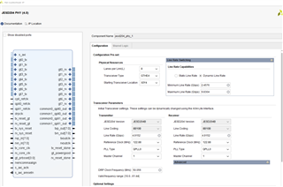
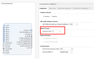
I am using Xilinx's JESD IP. The line rate is 4.9152Gbps, Lanes per Link is 8.
I have the following questions:
1. The AFE chip has 4 syncin pin and 4 syncout pin. Which pin should I connect to the corresponding FPGA JESD tx/rx Sync pin?
2. When AFE uses 8 lanes, how many JESD IPs should I use on the xilinx FPGA? One pair of tx/rx IP, or two pairs?
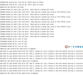
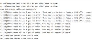
By the way: When I execute the "checkDeviceHealth" function, there is this error: ERROR:DAC JESD RX AB. Link Not Up. Didn't pass CS State. ERROR:SerDes Rx Lane 0 got LOS error. There may be a SerDes Eye issue.