This thread has been locked.

If you have a related question, please click the "Ask a related question" button in the top right corner. The newly created question will be automatically linked to this question.

AFE7950: Using EVM, getting no DAC output

Part Number: AFE7950

Sorry for the repost, but I'm not sure using the "ask related question" option worked because I got no responses.

Using the AFE7950EVM with TSW14J57 generator/capture board:

I have a programmable supply on both the AFE7950EVM, set at 5.5V (and it doesn't droop; at the test point even when drawing about 3 amps, it stays at 5.5V) and 12V going into the TSW14J57 board.

running through the tutorial ppt slides, I'm not getting any errors, and PLL2 Locked stays lit, but the TSW board D2 led only flashes during programming, and keeps flashing after running the S1 script. However, it goes out when i hit the "send" button in the DAC screen of the HSDC Pro software. I get no output from TXA on the AFE board (or any of the TX), and the only connection I've made is from the SMA connector at TXA to a spectrum analyzer. My SA has a BW of 7.5GHz and I'm not seeing anything, no matter where I zoom in. The SA has an input impedance of 50 ohms and its noise floor is at about -80dBm.

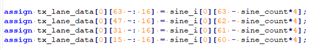
I'm not getting any JESD errors and don't have to run the AFE.adcDacSync() command, though I've tried without and with running that.

D3 (PLL2 locked) is on. The tutorial doesn't talk about it, but D4 on the AFEEVM (LMK locked) never comes on. not sure what thats for, but I'm guessing it's maybe just for when an ext 10MHz sync clock is used.

As I said, on the TSW board, after running S1 but *before* hitting the Send button in HSDC Pro, D2 is blinking, D3 is on and steady, D5 and D6 are on but dim? (maybe meaning they're actually flashing at hf), D8 and D9 are on. The rest (D1, D4, D7) are off. On the AFE EVM board, *only* D3 (pll2 locked) is on.

As soon as I hit send (per the last post, I was told the tutorial was incorrect in stating that I should hit send before running the S1 script), on the TSW board, D1 (TX sync) flashes momentarily, and D2 turns off, and stays off. D3 remains on.

I get no signal on the TXA output. again, I have no other wires connected, on the coax from TXA to my spectrum analyzer.

  • Hi David,

    On the AFE EVM LED D3 should be on after running the S1 script and D4 will only turn on when providing an ext 10MHz reference to LMK_CLK_IN, J14. 

    Below is the status of the J57 LEDs at different stages of the bringup:

    1. After selecting the INI file and loading firmware

      1. D1, D3, D8,D9 are all on (D5,D6 are on but dim). The rest (D2, D4, D7) are off.
    2. After pressing 'Send'
      1. D1, D3, D5, D6, D8,D9 are on. The rest are off.
    3. After running the Latte script D5 and D6 should immediately turn off and once the script is done the LEDs should be set as below.
      1. D2 should be flashing. D3, D6, D8, D9 should be on. All others (D1, D4, D5, D7) should be off. 

    Can you check if this matches what you see in your setup? If this does not match then the issue may be with the TSW14J57. To test if the AFE is being configured correctly and receiving all the necessary clocks, you can set the DAC into constant test pattern mode by adding the below lines to the very end of your script. With these lines added your will see an output at exactly the NCO frequencies. This will tell us that the AFE EVM is operating as expected and the issue seems to be with the TSW board. 

    for i in [0,1]:
    	for j in [0,1]:
    		AFE.JESD.DACJESD[i].dacJesdConstantTestPatternValue(1,j,0,16384,0) # enable, channelNum, bandNum, Ival, Qval

    Regards,

    David Chaparro

  • Thanks for the info. I was able to determine that the problem is the TSW board. I also ran the JESD loopback script that's provided with the AFE design files and that worked. I then loaded the ZCU102 design TI provides and that worked. So the AFE board itself seems to be working fine.

    I'm guessing I've had the TSW board for way too long to return it, but since I have the ZCU102 eval board working with the AFE board, can you tell me how to integrate the demo project into a larger project? Right now it's coded to just use a sine wave generator but I have samples that I need to send in real time, not from a preconfigured script. The synthesized project just gives connections needed for clock and JESD lanes, but i need a way to send real sample values up to the DAC instead of the sine wave array values.  Vivado doesn't allow dropping an SV file into a block design as a module, and I don't know how to write it as verilog. Is there a guide for integrating the example design into a larger fpga project?

  • Hi David,

    What we provide with these reference designs is a basic design that includes a ILA to view the captured data and a 64 point sine wave to send to the AFE. This was designed this way so that you could easily replace the ILA and 64 point sine wave with your custom logic and tone/pattern. 

    To change the tone that is being sent you should modify the refdesign_tx.sv file so that instead of putting the 64 point sine wave data onto the lanes you put your custom tone. Section 6.5 of the TI204c-IP Users Guide covers how to map Rx/Tx lane data to ADC/DAC samples. 

    Regards,

    David Chaparro

  • Just to verify before I dive any further into this: I'm not using the DAC to generate anything related to sine waves or IQ modulation. I just have "data" being loaded into RAM and I want the value of those ram words to drive the DAC output level, using the same clock that's putting the data in RAM to be the clock that updates the DAC output. I'm not sure how DUC/DDC works, but my understanding is that the DAC outputs whatever data values it's given at a rate equal to the NCO frequency. Is that right? So if my RAM values are loaded at a rate of 100MHz (or 200MBps or 1.6Gbps for 16-bit words, not including latency from inter-word delay) and the NCO is 2000MHz then the DAC is oversampling and outputing the memory values at 2GSps or each RAM word is output 10X per RAM clock cycle, right?

    I then want to use the ADC to read the values back in, such that the ADC buffer values are equivalent to the RAM values sent to the DAC.

    Does that make sense and is that right and will that work? I believe this is the equivalent to PAM modulation with 65536 levels. Since my RAM will actually only have 16 unique values (4 bit resolultion stored as the MSBs of the 16bit word) what I'm actually trying to do is create PAM-16 at 100MBaud