This thread has been locked.

If you have a related question, please click the "Ask a related question" button in the top right corner. The newly created question will be automatically linked to this question.

ADC12DJ5200RF EVM GUI setting

Other Parts Discussed in Thread: ADC12DJ5200RF, LMK04828, LMX2594, ADC12DJ5200RFEVM, LMK00304, LMK61E2

Hi 

I used ADC12DJ5200RF EVM GUI . and it does not connect with FPGA EVM.

FOLLOWING PIC1 JMODE 1 SETTING , jesd204C's block SERDES PLL LOCKED light on .

but PIC2 JMODE 2 SERDES PLL LOCKED doesn't light on .

what is the different?

and what is the meaning of SERDES PLL LOCKED ?

PIC1 :

PIC2 : 

  • Hello,

    The SERDES PLL LOCK bit means that the serializer PLL is locked, the serializer PLL is what sets the SERDES rate frequency.

    I can see that you are using on board clocking mode for the EVM, can you confirm that you made all of the necessary hardware changes listed on page 20 of the EVM user guide .

    If so can you verify using an oscope that the FPGA reference frequencies coming out of the LMK04828 match what is called for in the EVM GUI.

    Best,

    Eric

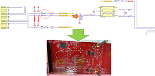
  • fellowing  PIC1 is my setting value. but LMX2594's output RFOUTAP(RFOUTAM) and RFOUTBP(RFOUTBM) did not have signal. the signal level always high.

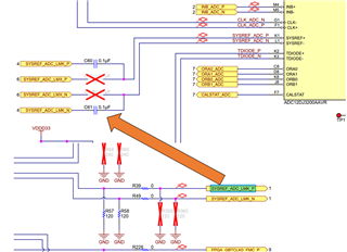
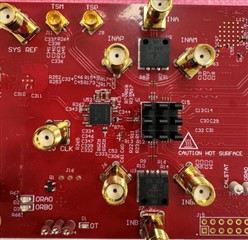
    I changed another way fellowing PIC2 and PIC3.

    Can I use FPGA_CLKA_FMC_P and SYSREF_ADC_LMK_P to be ADC input signals?

    PIC1 : 

    PIC2 : 

    PIC3:

  • Hello,

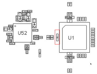
    Can you first confirm that you have made the following hardware changes, specifically...

    • removing C2 and C3, populating R171 and R174
    • removing C60 and C61, populate C52 and C306
    • Uninstall Jumper J13

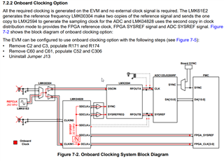
    These changes are required to make on board clocking work. You can also take a look at the block diagram below.

    Unless you have a very high frequency scope you will not be able to see the RFOUTA of the LMX2594, you should be able to see the RFOUTB signal of the LMX2594 but this signal might also be to high a frequency depending on what type of scope you have.

    I am not sure what you are trying to do in picture 2 but I would not recommend it. If you follow the changes I suggested above you will have a much easier time getting the ADC to run with the onboard clocks.

    I am also not sure what picture 3 is trying to show can you elaborate please?

    I would not recommend using FPGA_CLKA_FMC_P and SYSREF_ADC_LMK_P to be ADC input signals.

    Thanks,

    Eric

  • Hi sir : 

    I can not find the C2 and C3.

    Could you tell me where is it?

  • Hello,

    Please check the ADC ASSY document in the design file download for the exact location it is tough to tell but C2 and C3 are the capacitors right next to the ADC. See screen shot below.

    Best,

    Eric

  • Hi Sir : 

    I fellow PIC1 setting and PIC2 , but LMX2594 RFOUTA and RFOUTB that I can not measure any singal (only pull high level).

    Idealy ,it must be measured 100MHz(clk) and 3.125MHz(sysref)

    Is there anything i can do?

    PIC1 :

    PIC2 : 

  • Hello,

    Please see my previous comments about measuring the LMX output, 

    Unless you have a very high frequency scope you will not be able to see the RFOUTA of the LMX2594, you should be able to see the RFOUTB signal of the LMX2594 but this signal might also be to high a frequency depending on what type of scope you have.

    RFOUTA is the sampling frequency that you supply to the ADC, it will be 1000MHz based on what you are programming in the GUI PIC you shared.

    If you want to try and probe clock signals try the ones coming out of the LMK04828, these will be much lower frequency and you should be able to probe these. How are you taking these measurements, are you using an oscilloscope? If so what is the bandwidth of the scope. 

    Also are you able to capture data and display it?

     Best,

    Eric

  • Hi Eric : 

    I used onboard clocking option.  

    I Follow the adc12dj5200RFEVM instruction : 

    ->Remove C2 and C3, populate R171 and R174 

    ->Remove C60 and C61, populate C52 and C306  

    ->Uninstall Jumper J13

    I set the EVM GUI user input : JMODE2 , Fs selection : 1000Msps.

    I use the scope model is RTM3044 . I am able to see the signal FPGA_CLKB_FMC_P (100MHz) and FPGA_SYSREF_FMC_P (3.125MHz) (from LMK04828).

    Following the datasheet page 19 (onboard clocking option) onboard clocking system block diagram LMK04828 output to LMX2594's input (SYNC , SYSREFREQ :3.125MHz) , but i can not see the LMX2594's RFOUTA and RFOUTB.

    The signals which  LMX2594's RFOUTA and RFOUTB to ADC12DJ5200's input . and this two signal must be same value with FPGA's FPGA_SYSREF and FPGA_CLK.

    so i can not see the serdes pll locked light turn on.  but i change JMODE1 the serdes pll locked light turn on.

    i don't know what the different?

  • Hello,

    The fact you are able to measure the the FPGA_CLK and FPGA_SYSREF correctly mean that the LMK04828 is being setup correctly.

    As I have said in my previous messages unless you have a very high bandwidth scope (which the RTM3044 is not I think only 100MHz of bandwidth you will not be able to see the signal) The RFOUTA of the LMX2594 is set to 1GHz the sampling clock of the ADC, based on the scope you have you will not have enough bandwidth to measure this signal. The RFOUTB channel of the LMX2594 is powered down by default as this output is just used for sysref and that is not needed. 

    One thing you could probe is the the OSCIN of the LMX2594 coming out of the LMK00304 this should be 100MHz CLKOUTA of this chip will go to the LMX and CLKOUTB will go to the LMK04828. They should both be 100MHz.

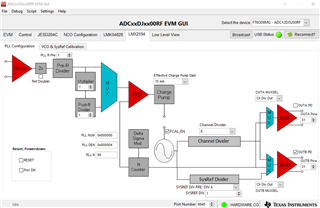
    The LMX will take this reference signal and multiply it up using a pll to the correct sampling frequency, after you program the adc evm using the gui check the LMX2594 tab of the gui and make sure it looks like this. 

    We can calculate the output at Channel A by doing the following OSCIN = 100MHz, PLL N = 80, Channel divider = 8

    OSCIN*PLL_N/channel_divider = 100 MHz * 80 / 8 = 1000MHz = 1GHz.

    The problem you are seeing with the SERDES PLL lock not turning on means that the part is likely not getting the correct sampling clock frequency, I would double check these settings I showed you and make sure they are all right.

    Best,

    Eric

  • Hi Eric : 

    thank you that you can help me to check the setting what i did.

    another question is about you said The RFOUTB channel of the LMX2594 is powered down by default as this output is just used for sysref and that is not needed. Whether  ADC12DJ5200RF needs the signal SYSREF or not?

    I turn off OUTB PD and i didn't see the signal on LMX2594's RFOUTB. Does that mean signal frequency too high?

    and Would you tell me how calculate the sysref ?

  • Hello,

    The ADC does not need sysref to function by default so you can leave that off for operation. If you want to turn it on you can do as you have done and enable it, to change the frequency you can increase the dividers you see on that path for RFOUTB. The way it is set by default is OSCIN*PLL_N/SYSREF_DIV_PRE/SYSREF_DIV gives us 100MHz*80/4/1 = 2000 MHz. If you want to lower this frequency increase the SYSREF_DIV dropwdown you could set it to 64 for example and you should see an output of 31.25 MHz. You can also play with the OUTB Pow dropdown to increase the signal strength.

    Were you able the verify the OSCIN signal of the LMX2594?

    Thank you,

    Eric

  • Hi Eric : 

    The OSCIN signal of the LMX2594 is 100MHz under the setting JMOD2 / 1000Msps.

  • Ok,

    are you able to capture data now?

  • Hi Eric : 

    No , I can't.

    ADC12DJ5200RF EVM connect with KCU105 EVM.

    But I can't see the signal rx_sync (jesd204 IP (XILINX)) turns on.

    I'm sure whether the RX_JESD204 doesn't receive the data from ADC EVM.

  •  I am not sure what you mean by "I'm sure whether the RX_JESD204 doesn't receive the data from ADC EVM." can you elaborate? Are you able to put the ADC into transport layer test pattern mode and see what you get if it matches to table 7-60.

  • Hi sir :

    following picture1 serdes rate is the line rate?

    How do I calculate the JESD204's reference clock?

    picture1:  (AD12DJ5200RF)

  • Hi Sir :100 

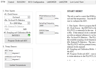
    I use JMOD31 and  GUI's FPGA Reference clock is 100MHz. (following picture 1)

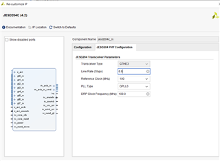
    I use the XILINX FPGA JESD204 IP but i can't find the reference clock is 100MHz (following picture 3).

    so i have to adjust the LMK04828 output clock to match the IP , but the problem is that i can't multiple frequency bigger than 100MHz.

    what should I do ?


    picture 1 :

    picture 2 : 

    picture 3 : 

  • What I would do instead of adjusting the LMK dividers you can keep them at 1 which essentially means you are going to just bypass the signal you input at the CLCKIN_1 pin of the LMK04828. Then you can program the LMK61E2 to the reference frequency you desire in your case 200 MHz it looks like based on the screenshot you provided. The one thing you will have to watch out for is that after you change the frequency output from the LMK61E2 you will also have to adjust the divider settings on the LMX2594 so that you still get the correct sampling frequency to the ADC. This image below shows how all the clocks work. In onboard clocking mode the LMK61E2 provides the reference to both the LMK04828 (used for generating FPGA clock signals) and the LMX2594 (To generate the adc sample clock)

    Best,

    Eric 

  • Hi Sir : 

    (1) Does the  picture 1 SERDES rate is the same as picture 2 line rate?

    (2) How do I calculate the FPGA Reference clock in different Fs?

    picture 1 : 

    picture 2 : 

  • Hello,

    1) Yes the SERDES rate is the same as line rate.

    2) There are two clocks required to be sent to the FPGA, the FPGA ref clock for the JESD IPs application facing side for samples and SYSREF releated timing this has strict requirements based on your JESD PHYs width i.e 32 bit 64 bit 128 bit. The other clock is the GBTCLK for the PHY in the FPGA to generate the line rate frequency required by the JESD link, this clock has less restrictions. 

    The FPGA ref clock has the following requirements depending on encoding type...

     in 8b10b modes

    fpga ref clock = Linerate/80, this is true if the PHY is set to deserialize each lane to 64 bits

    fpga ref clock = Linerate/40, this is true if the PHY is set to deserialize each lane to 32 bits

    in 64b66b modes

    fpga ref clock = linerate/66, this is true if the PHY is set to deserialize each lane to 64 bits

    fpga ref clock = linerate/33, this is true if the PHY is set to deserialize each lane to 32 bits

    fpga ref clock = linerate/132, this is true if the PHY is set to deserialize each lane to 128 bits this is also required for line rates above 16 Gbps


    Typically we just follow linerate/80 for 8b10b modes and linerate/66 for 64b66b modes as our phy has a width of 64 bits. However, you can change this to fit your clock requirement as you see fit. These fpga ref clocks can be multiplied by any integer to meet your requirements and should still work. For the GBTCLK the main requirement is keeping it within the FPGA VCO range to generate the linkrate clock required. Typically we set this to match the FPGA ref clock frequency.

    So in your case you show above equations to calculate SERDES rate and FPGA ref clock rate would be

    Fs = 2000 Msps

    SERDES rate = Fs*r in this case r = 3.3, this value can be found in the operating modes table on page 96, this is specific for just this JMODE

    so SERDES rate = 6600 MSps

    FPGA ref clock is equal to SERDES rate by 66

    FPGA ref clock = SERDES/66 = 6600/66 = 100 MHz

    Hope this helps,

    Eric

  • Hi Sir : 

    (1) Does the ADC12DJ5200RF 's reference clock is the same as xilinx JESD IP's core clock? following picture 1.

    picture 1 : 

  • Hello,

    sorry for the delayed response, yes this is the same. If you are having trouble creating the JESD link in the fpga we offer custom JESD ip firmware you can use, if you would be interested in this let me know.

    Best,

    Eric

  • Hi Sir : 

    Could you show me how to ued xilinx JESD IP and line to ADC12DJ5200?

  • Hello,

    I can not support Xilinx JESD IP, we can offer you TI JESD IP. This I can help with.

    Best,

    Eric