- Ask a related questionWhat is a related question?A related question is a question created from another question. When the related question is created, it will be automatically linked to the original question.
Hi
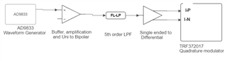
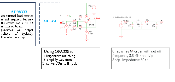
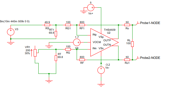
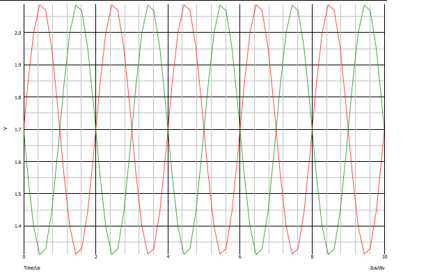
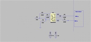
we design a PCB with TRF372017 , a waveform generator IC ( AD9833) will be used to generate BB waveform, a 5th order Chepyshev LPF shall be used after AD9833 as a reconstruction filter to eliminate harmonics, then Unipolar to bipolar converters, and finally using high speed differential amplifier to convert single-Ended to Diff, and provide a DC shift to 1.7V as a Vcom to be suitable for TRF372017 with( Vp-p) almost 1V as shown in next Fig.
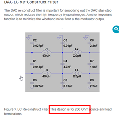
so after all, we have a differential signal with Bias 1.7 V and almost 0.3 Vrms as in datasheet and the reconstruction filter already applied at the beginning.
i can't find an example for circuit to connect op-amp differential output with input baseband pins of TRF372017.
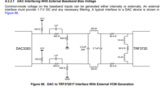
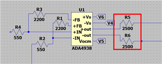
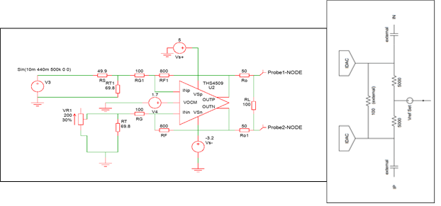
According to TRF372017 datasheet figure 86 "DAC to TRF372017 Interface With External VCM Generation". I have these questions:
1-could I use this configuration to connect op-amp differential outputs to TRF372017 BB directly or need modifications ?
2- is this configuration suitable for Wideband applications, can explain this configuration
3- how can make output impedance of differential op amp match with input impedance of IQ modulator (5K) ohm?
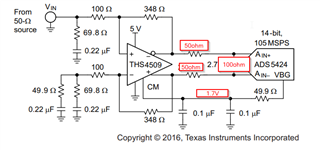
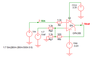
4- can i use following circuit to drive BB of IQ modulator? (like this technical article https://www.analog.com/en/technical-articles/baseband-design-example-for-ltc5589-ltc5599-low-power-iq-modulator.html
I tried hard, i have read. TRF372017, DAC3283, SLUA647A but all discuss another case
Appreciate your support.
regards
Eng. maged