This thread has been locked.

If you have a related question, please click the "Ask a related question" button in the top right corner. The newly created question will be automatically linked to this question.

AFE7900EVM: TI IP RX Side not working.

Part Number: AFE7900EVM
Other Parts Discussed in Thread: AFE7950

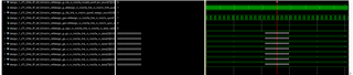
Hi, I am using the TI IP on a Kintex Ultrascale Board with AFE7950. The problem I am facing is that no data is shown on the ILA of the TI IP after I run the Ramp Test Pattern on Latte. The lanes are syncing, but no data is displayed on the ILA. I have attached the Latte script, block diagram, TI IP parameters, and a screenshot of the ILA below.

Latte Script:


setupParams.skipFpga 				= 1
sysParams							=	AFE.systemParams
setupParams.fpgaRefClk 				= 122.88
#setupParams.fpgaRefClk 				= 245.76	
#setupParams.fpgaRefClk 				= 256.00
AFE.systemStatus.loadTrims			= 1

sysParams.FRef                    	= 491.52
sysParams.FadcRx                  	= 2949.12
sysParams.FadcFb				  	= 2949.12
sysParams.Fdac                    	= 2949.12 * 3
#sysParams.FRef                    	= 512
#sysParams.FadcRx                  	= 3072
#sysParams.FadcFb				  	= 3072
#sysParams.Fdac                    	= 3072*3

#sysParams.rxEnable                  =   [True,False,False,False]
sysParams.rxEnable		            =	[True,True,True,True]
sysParams.txEnable                  =   [True,True,True,True]
sysParams.enableDacInterleavedMode	= False 					#DAC interleave mode to save power consumption. Fs/2 - Fin spur occurs

sysParams.modeTdd 					= 0		
										# 0- Single TDD Pin for all Channels
										# 1- Separate Control for 2T/2R/1F
										# 2- Separate Control for 1T/1R/1F			

sysParams.topLevelSystemMode		= 'StaticTDDMode'
sysParams.RRFMode 					= 0   #4T4R2F FDD mode
#sysParams.jesdSystemMode			= [0,0]
sysParams.jesdSystemMode			= [3,3]
										#SystemMode 0:	2R1F-FDD						; rx1-rx2-fb-fb
										#SystemMode 1:	1R1F-FDD						; rx1-rx1-fb-fb
										#SystemMode 2:	2R-FDD							; rx1-rx1-rx2-rx2
										#SystemMode 3:	1R								; rx1-rx1-rx1-rx1
										#SystemMode 4:	1F								; fb-fb-fb-fb
										#SystemMode 5:	1R1F-TDD						; rx1/fb-rx1/fb-rx1/fb-rx1/fb
										#SystemMode 8:	1R1F-TDD 1R-FDD	(FB-2Lanes)(RX1 RX2 interchanged)		; rx2/fb-rx2/fb-rx1-rx1


sysParams.jesdLoopbackEn			= 0 #Make it 1 to Enable the JESDTX to JESDRX internal loopback
#sysParams.LMFSHdRx                	=['12410', '12410', '12410', '12410']
sysParams.LMFSHdRx                	=['44210', '44210', '44210', '44210']
#sysParams.LMFSHdRx                	=['14810', '14810', '14810', '14810']
										# The 2nd and 4th are valid only for jesdSystemMode values in (2,6,7,8). For other modes, select 4 converter modes for 1st and 3rd.
sysParams.LMFSHdFb                	= ["22210","22210"]
#sysParams.LMFSHdTx                	= ["24410","24410","24410","24410"]
sysParams.LMFSHdTx                	= ["12410","12410","12410","12410"]
#sysParams.LMFSHdTx                	= ["44210","44210","44210","44210"]
sysParams.jesdTxProtocol            = [0,0]
sysParams.jesdRxProtocol            = [0,0]
sysParams.serdesFirmware			= True 		# If you want to lead any firmware, please speify the path here. Otherwise it will not write any firmware
#sysParams.jesdTxLaneMux				= [0,1,2,3,4,5,6,7]	
sysParams.jesdTxLaneMux					= [4,5,6,7,3,0,1,2]
												# Enter which lanes you want in each location. 
												# Note that across 2T Mux is not possible in 0.5.
												# For example, if you want to exchange the first two lines of each 2T, this should be [[1,0,2,3],[5,4,6,7]]
sysParams.jesdRxLaneMux				= [0,1,2,3,4,5,6,7]	
												# Enter which lanes you want in each location.
												# Note that across 2R Mux is not possible in 0.5.
												# For example, if you want to exchange the first two lines of each 2R, this should be [[1,0,2,3],[5,4,6,7]]
#sysParams.txDataMux					= [2,3,0,1,4,5,6,7]
sysParams.txDataMux					= [0,1,2,3,4,5,6,7]

sysParams.jesdRxRbd					= [4, 4]
sysParams.jesdTxRbd					= [1, 1]

sysParams.rxJesdTxScr				= [False,False,False,False]
sysParams.fbJesdTxScr				= [False,False]
sysParams.jesdRxScr					= [False,False,False,False]

sysParams.rxJesdTxK					= [32,32,32,32]
sysParams.fbJesdTxK					= [32,32]
sysParams.jesdRxK					= [32,32,32,32]

sysParams.ncoFreqMode 				= "1KHz"
	
sysParams.txNco0					= 	[[800,800],		#Band0, Band1 for TxA for NCO0
										[800,800],        #Band0, Band1 for TxB for NCO0
										[800,800],        #Band0, Band1 for TxC for NCO0
										[800,800]]        #Band0, Band1 for TxD for NCO0


sysParams.rxNco0					= 	[[800,800],		#Band0, Band1 for RxA for NCO0
										[800,800],        #Band0, Band1 for RxB for NCO0
										[800,800],        #Band0, Band1 for RxC for NCO0#
										[800,800]]        #Band0, Band1 for RxD for NCO0

#sysParams.rxNco0					= 	[[200,200],		 #Band0, Band1 for RxA for NCO0
#									[200,200],        #Band0, Band1 for RxB for NCO0
#									[200,200],        #Band0, Band1 for RxC for NCO0
#									[200,200]]        #Band0, Band1 for RxD for NCO0


sysParams.fbNco0					= 	[2600,2600]			#FBA, FBC for NCO0


sysParams.numBandsRx				= [0]*4					# 0 for single, 1 for dual
sysParams.numBandsFb				= [0,0]				
sysParams.numBandsTx				= [0,0,0,0]

sysParams.ddcFactorRx             	= [24,24,24,24]			# DDC decimation factor for RX A, B, C and D
#sysParams.ddcFactorRx             	= [12,12,12,12]			# DDC decimation factor for RX A, B, C and D
sysParams.ddcFactorFb             	= [6,6]
#sysParams.ducFactorTx             	= [36,36,36,36]
sysParams.ducFactorTx             	= [72,72,72,72]

## The following parameters sets up the LMK04828 clocking schemes
lmkParams.pllEn						=	True#False
lmkParams.inputClk					=	1474.56#737.28
#lmkParams.inputClk					=	1536.00
lmkParams.sysrefFreq				=	3.84
#lmkParams.sysrefFreq				=	1.92
lmkParams.lmkFrefClk				=	True

## The following parameters sets up the register and macro dumps
logDumpInst.setFileName(ASTERIX_DIR+DEVICES_DIR+r"\Afe79xxPg1.txt")
logDumpInst.logFormat				= 0x00
logDumpInst.rewriteFile				= 1
logDumpInst.rewriteFileFormat4		= 1
device.optimizeWrites				= 0
device.rawWriteLogEn				= 1

## The following parameters sets up the SYNCIN and SYNCOUT to interface with the TSW14J57
sysParams.jesdABLvdsSync			= 1
sysParams.jesdCDLvdsSync			= 1
sysParams.rxJesdTxSyncMux			= [0,0,0,0]
sysParams.fbJesdTxSyncMux			= [0,0]
sysParams.jesdRxSyncMux				= [0,0,0,0]		#[0,0,1,1]
sysParams.syncLoopBack				= True

## The following parameters sets up the AGC
#sysParams.agcParams[0].agcMode = 1 ##internal AGC
#sysParams.agcParams[0].gpioRstEnable = 0 ##disable GPIO based reset to AGC detector 
#sysParams.agcParams[0].atken = [0, 1, 0] ##enable big and small step attack
#sysParams.agcParams[0].decayen = [0,1,0] ##enable big and small step decay
#sysParams.agcParams[0].atksize = [2,1,0] ## bigs step = 2dB, small step = 1dB
#sysParams.agcParams[0].decaysize = [2,1,0] ##big step = 2dB, small step = 1dB
#sysParams.agcParams[0].atkthreshold = [-1, -2, -14] ##attack threshold
#sysParams.agcParams[0].decaythreshold = [-14, -6, -20] ##decay threshold
#sysParams.agcParams[0].atkwinlength = [170, 170] ## detector time constant expressed inn absolute time in ns. 
#sysParams.agcParams[0].decaywinlength = 87380 ##detector time constant expressed in absolute time in ns. All detectors use the same value for decay time constant
#sysParams.agcParams[0].atkNumHitsAbs = [8,8] ##absolute number of times signal crosses threshold. These crossing are with respect to the FADC/8 clock
#sysParams.agcParams[0].decayNumHitsAbs = [100,100] ##absolute number of times signal crosses threshold. These crossing are with respect to the FADC/8 clock
#sysParams.agcParams[0].minDsaAttn = 0 ##minimum DSA attenuation used by AGC
#sysParams.agcParams[0].maxDsaAttn = 22 ##maximum DSA attenuation used by AGC
#sysParams.agcParams[0].totalGainRange = 22 ##total gain range used by ALC for gain compensation
#sysParams.agcParams[0].minAttnAlc = 0 ##minimum attenuation used by ALC for compensation when useMinAttnAgc = 0
#sysParams.agcParams[0].useMinAttnAgc = 1 ##enable ALC to use minimum attenuation from AGC for which compensation is required.
#sysParams.agcParams[0].alcEn = 1
#sysParams.agcParams[0].alcMode = 0 ##floating point DGC
#sysParams.agcParams[0].fltPtMode = 0 ##if exponent > 0, dont send MSB
#sysParams.agcParams[0].fltPtFmt = 1 ##3 bit exponent


## The following parameters sets up the GPIOs
sysParams.gpioMapping={
		'H8': 'ADC_SYNC0',
		'H7': 'ADC_SYNC1',
		'N8': 'ADC_SYNC2',
		'N7': 'ADC_SYNC3',
		'H9': 'DAC_SYNC0',
		'G9': 'DAC_SYNC1',
		'N9': 'DAC_SYNC2',
		'P9': 'DAC_SYNC3',
		'P14': 'GLOBAL_PDN',
		'K14': 'FBABTDD',
		'R6': 'FBCDTDD',
		'H15': ['TXATDD','TXBTDD'],
		'V5': ['TXCTDD','TXDTDD'],
		'E7': ['RXATDD','RXBTDD'],
		'R15': ['RXCTDD','RXDTDD']}
		
#AFE.systemParams.papParams[0]['enable'] = True
#AFE.systemParams.papParams[1]['enable'] = True
#AFE.systemParams.papParams[2]['enable'] = True
#AFE.systemParams.papParams[3]['enable'] = True
		

## Initiates LMK04828 and AFE79xx Bring-up
setupParams.skipLmk	=	False

AFE.initializeConfig()
lmkParams.sysrefFreq = AFE.systemStatus.sysrefFreq
lmkParams.lmkPulseSysrefMode = False
AFE.LMK.lmkConfig()
## Initiates AFE79xx Bring-up
setupParams.skipLmk	=	True
AFE.deviceBringup()

AFE.TOP.overrideTdd(15,0,15)
#AFE.JESD.ADCJESD[0].adcRampTestPattern(0,1,0)
#AFE.JESD.ADCJESD[0].adcRampTestPattern(1,1,0)
#AFE.JESD.ADCJESD[1].adcRampTestPattern(0,1,0)
#AFE.JESD.ADCJESD[1].adcRampTestPattern(1,1,0)

#AFE.JESD.DACJESD[0].dacJesdConstantTestPatternValue(1,0,0,16384,0)
#AFE.JESD.DACJESD[0].dacJesdConstantTestPatternValue(1,1,0,16384,0)

#AFE.JESD.DACJESD[1].dacJesdConstantTestPatternValue(1,0,0,16384,0)
#AFE.JESD.DACJESD[1].dacJesdConstantTestPatternValue(1,1,0,16384,0)

Block Diagram:

Ila:

TI IP Parameters:

`undef IP_8B10B
`undef IP_64B66B
`define IP_8B10B


`undef IP_TYPE
`define IP_TYPE "RXTX"

`undef ADC_RESOLUTION
`define ADC_RESOLUTION 16

`undef DAC_RESOLUTION
`define DAC_RESOLUTION 16

`undef NUMBER_OF_RX_LANES
`undef NUMBER_OF_TX_LANES

`define NUMBER_OF_RX_LANES 8
`define NUMBER_OF_TX_LANES 8


`undef NUMBER_OF_QUADS
`define NUMBER_OF_QUADS 2


`undef MGT_TYPE
`define MGT_TYPE "GTH"


`undef NUMBER_OF_REFCLK_BUFFERS
`define NUMBER_OF_REFCLK_BUFFERS 1


`undef LANE_ADC_TO_GT_MAP
`define LANE_ADC_TO_GT_MAP {5,4,6,7,3,0,1,2}

`undef LANE_DAC_TO_GT_MAP
`define LANE_DAC_TO_GT_MAP {4,5,6,7,3,0,1,2}


`undef RX_LANE_POLARITY
`define RX_LANE_POLARITY 8'b00110011

`undef TX_LANE_POLARITY
`define TX_LANE_POLARITY 8'b00001111


`undef RX_LANE_DATA_WIDTH
`define RX_LANE_DATA_WIDTH 64


`undef TX_LANE_DATA_WIDTH
`define TX_LANE_DATA_WIDTH 64


`undef RX_F_VAL
`define RX_F_VAL 2

`undef TX_F_VAL
`define TX_F_VAL 2


`undef RX_K_VAL
`define RX_K_VAL 16

`undef TX_K_VAL
`define TX_K_VAL 16


`undef RBD_COUNT_WIDTH
`define RBD_COUNT_WIDTH 10


`undef RX_BUFFER
`define RX_BUFFER "NORM"

`undef BUFFER_RATIO
`define BUFFER_RATIO 1

`undef TX_BUFFER
`define TX_BUFFER "NORM"

  • Hi Muhammad,

    Can you confirm that the rx link has been taken out of reset and that the link has been established? In the Vivado hw_vios tab set rx_sync_reset_vio to 0. A successful Rx link will be indicated by the ‘rx_lmfc_to_buffer_release_delay’ parameter updating.

    Regards,

    David Chaparro

  • Hi David, 

    The rx link has been released from reset. I've set rx_sync_reset_vio to 0, and the parameter for rx_lmfc_to_buffer_release_delay updates its value. When rx_sync_reset_vio is set to 1, the rx_sync_n signal in the ilareflects a value of 1. However, upon updating the signal to 0, the rx_sync_n signal also updates its value to 0, as evident in the attached ila screenshot.

    Regards,

    Muhammad Umer

  • Hi Muhammad,

    When the rx_sync_reset_vio is set to 0 do you see any data on the lanes or is it always 0? If always 0 can you share the 'TI_204C_IP_ref.sv' and 'refdesign_rx.sv' documents so I can check for any possible issues?

    Can you try enabling the ramp pattern for all channels using the lines below? 

    for i in range(3):
    	AFE.JESD.ADCJESD[0].adcRampTestPattern(i,1,1)
    	AFE.JESD.ADCJESD[1].adcRampTestPattern(i,1,1) #chNo, En, RampInc 

    Regards,

    David Chaparro

  • Hi David, 

    The data on the lanes is always 0. I have attached the documents that you have requested, please review them. I have also tried enabling the ramp pattern on all the lanes, but the value is always 0.

    refdesign_rx.sv

    `default_nettype none
    `timescale 1ps/1ps
    
    module refdesign_rx
    #(
    	parameter IP_PROTOCOL = 810,
    	parameter NUM_RX_LANES = 8,
    	parameter RX_LN_DATA_WIDTH = 64,
    	parameter ADC_RES = 16
    	)
    (
    // Free running clock required by the transceiver
    	input wire	mgt_freerun_clock,
    
    // Application/System Clock for the Rx
    	input wire	rx_sys_clock,
    
    // Application/System Synchronous Reset for the Rx
    	input wire	rx_sync_reset,
    
    	input wire rx_all_lanes_locked,
    	input wire rx_release_all_lanes,
    
    // Lane data outputs. There is one output data
    // bus per lane
    	input wire	[RX_LN_DATA_WIDTH-1:0] rx_lane_data [NUM_RX_LANES-1:0],
    
    // Data valid signal. This applies simultaneously
    // to all lanes
    	input wire	rx_lane_data_valid,
    
    // Rx Lane Buffer overflow indicator
    	input wire	[NUM_RX_LANES-1:0] rx_lane_buffer_overflow,
    
    // SYNCn signal
    	input wire	rx_sync_n,
    
    	input wire	[111:0] rx_lane_configuration_data [NUM_RX_LANES-1:0],
    	input wire	[RX_LN_DATA_WIDTH/8-1:0] rx_lane_start_of_frame [NUM_RX_LANES-1:0],
    	input wire	[RX_LN_DATA_WIDTH/8-1:0] rx_lane_start_of_multiframe [NUM_RX_LANES-1:0],
    
    // The following are the lane sideband signals
    // in 64b/66b mode
    
    	input wire	[NUM_RX_LANES-1:0] rx_lane_start_of_mblock,
    	input wire	[NUM_RX_LANES-1:0] rx_lane_start_of_emblock,
    	input wire	[NUM_RX_LANES-1:0] rx_lane_crc_error,
    
    // The following signals are the error related
    // counts for the 8b/10b protocol
    	input wire	[3:0] rx_lane_invalid_somf_err_count [NUM_RX_LANES-1:0],
    	input wire	[3:0] rx_lane_invalid_eomf_err_count [NUM_RX_LANES-1:0],
    	input wire	[3:0] rx_lane_invalid_eof_err_count [NUM_RX_LANES-1:0],
    	input wire	[3:0] rx_lane_notintable_err_count [NUM_RX_LANES-1:0],
    	input wire	[3:0] rx_lane_disp_err_count [NUM_RX_LANES-1:0],
    
    // The following signals are the error related
    // counts for the 64b/66b protocol
    	input wire	[3:0] rx_lane_invalid_header_err_count [NUM_RX_LANES-1:0],
    	input wire	[3:0] rx_lane_invalid_eomb_err_count [NUM_RX_LANES-1:0],
    	input wire	[3:0] rx_lane_invalid_eoemb_err_count [NUM_RX_LANES-1:0],
    	input wire	[3:0] rx_lane_crc_mismatch_err_count [NUM_RX_LANES-1:0],
    
    // Rx Sysref control and status signals
    	input wire	rx_sysref,
    	input wire	[3:0] rx_sysref_realign_count,
    	input wire	rx_clr_sysref_realign_count,
    	input wire	rx_lmfc_pulse,
    	input wire	rx_lemc_pulse
    );
    
    /////////////////////////////////////////////
    // Instantiate the IP
    /////////////////////////////////////////////
    
    // Instantiate a VIO for reflecting the ILAS
    // config octets for each lane. This is valid
    // only for 8b/10b mode
    
    if (IP_PROTOCOL == 810)
    
    begin
    
    vio_ilas vio_ilas_inst (
    	.clk (mgt_freerun_clock),
    	.probe_in0 (rx_lane_configuration_data[0]),
    	.probe_in1 (rx_lane_configuration_data[1]),
    	.probe_in2 (rx_lane_configuration_data[2]),
    	.probe_in3 (rx_lane_configuration_data[3]),
    	.probe_in4 (rx_lane_configuration_data[4]),
    	.probe_in5 (rx_lane_configuration_data[5]),
    	.probe_in6 (rx_lane_configuration_data[6]),
    	.probe_in7 (rx_lane_configuration_data[7])
    	);
    
    end
    
    // Xilinx ILA module for capturing the Rx lanes and
    // their sideband signals
    // NOTE: This supports a max of 8 lanes
    ila_link_rx 
    #(
    	.LINK_PROTOCOL (IP_PROTOCOL),
    	.NUM_LANES (NUM_RX_LANES),
    	.RX_BYTES_PER_LANE (RX_LN_DATA_WIDTH/8)
    	)
    ila_link_rx_inst (
    	.sys_clock (rx_sys_clock),
    	.rx_lane_data (rx_lane_data),
    	.rx_lane_data_valid (rx_lane_data_valid),
    	.rx_lane_start_of_frame (rx_lane_start_of_frame),
    	.rx_lane_start_of_multiframe (rx_lane_start_of_multiframe),
    	.rx_lane_start_of_mblock (rx_lane_start_of_mblock),
    	.rx_lane_start_of_emblock (rx_lane_start_of_emblock),
    	.rx_lane_crc_error (rx_lane_crc_error),
    	.rx_lane_buffer_overflow (rx_lane_buffer_overflow),
    	.rx_lane_invalid_somf_err_count (rx_lane_invalid_somf_err_count),
    	.rx_lane_invalid_eomf_err_count (rx_lane_invalid_eomf_err_count),
    	.rx_lane_invalid_eof_err_count (rx_lane_invalid_eof_err_count),
    	.rx_lane_notintable_err_count (rx_lane_notintable_err_count),
    	.rx_lane_disp_err_count (rx_lane_disp_err_count),
    	.rx_lane_invalid_header_err_count (rx_lane_invalid_header_err_count),
    	.rx_lane_invalid_eomb_err_count (rx_lane_invalid_eomb_err_count),
    	.rx_lane_invalid_eoemb_err_count (rx_lane_invalid_eoemb_err_count),
    	.rx_lane_crc_mismatch_err_count (rx_lane_crc_mismatch_err_count),
    	.rx_sync_n (rx_sync_n),
    	.rx_sysref (rx_sysref),
    	.rx_sysref_realign_count (rx_sysref_realign_count),
    	.rx_lmfc_pulse (rx_lmfc_pulse),
    	.rx_lemc_pulse (rx_lemc_pulse)
    );
    
    // The following logic maps the output of the Rx
    // Transport Layer to an ILA (for signal analysis)
    
    // Logic for mapping Rx samples to channel data
    // In this reference design, the data output is as
    // follows:
    // Channel 1 outputs 16 bit I stream on Lane 0
    // Channel 1 outputs 16 bit Q stream on Lane 1
    // Channel 2 outputs 16 bit I stream on Lane 2
    // Channel 2 outputs 16 bit Q stream on Lane 3
    // Channel 3 outputs 16 bit I stream on Lane 4
    // Channel 3 outputs 16 bit Q stream on Lane 5
    // Channel 4 outputs 16 bit I stream on Lane 6
    // Channel 4 outputs 16 bit Q stream on Lane 7
    
    (*dont_touch = "true"*) wire [ADC_RES-1:0] ch1_I_samples[3:0];
    (*dont_touch = "true"*) wire [ADC_RES-1:0] ch1_Q_samples[3:0];
    (*dont_touch = "true"*) wire [ADC_RES-1:0] ch2_I_samples[3:0];
    (*dont_touch = "true"*) wire [ADC_RES-1:0] ch2_Q_samples[3:0];
    (*dont_touch = "true"*) wire [ADC_RES-1:0] ch3_I_samples[3:0];
    (*dont_touch = "true"*) wire [ADC_RES-1:0] ch3_Q_samples[3:0];
    (*dont_touch = "true"*) wire [ADC_RES-1:0] ch4_I_samples[3:0];
    (*dont_touch = "true"*) wire [ADC_RES-1:0] ch4_Q_samples[3:0];
    
    genvar i;
    generate for (i=0; i<4; i=i+1)
    begin : sample_gen
    
    assign ch1_I_samples[i] = rx_lane_data[0][63-16*i -: ADC_RES];
    assign ch1_Q_samples[i] = rx_lane_data[1][63-16*i -: ADC_RES];
    assign ch2_I_samples[i] = rx_lane_data[2][63-16*i -: ADC_RES];
    assign ch2_Q_samples[i] = rx_lane_data[3][63-16*i -: ADC_RES];
    assign ch3_I_samples[i] = rx_lane_data[4][63-16*i -: ADC_RES];
    assign ch3_Q_samples[i] = rx_lane_data[5][63-16*i -: ADC_RES];
    assign ch4_I_samples[i] = rx_lane_data[6][63-16*i -: ADC_RES];
    assign ch4_Q_samples[i] = rx_lane_data[7][63-16*i -: ADC_RES];
    
    end
    endgenerate
    
    ila_samples ila_samples_inst (
    	.clk (rx_sys_clock),
    
    	.probe0 (ch1_I_samples[0]),
    	.probe1 (ch1_I_samples[1]),
    	.probe2 (ch1_I_samples[2]),
    	.probe3 (ch1_I_samples[3]),
    	.probe4 (ch1_Q_samples[0]),
    	.probe5 (ch1_Q_samples[1]),
    	.probe6 (ch1_Q_samples[2]),
    	.probe7 (ch1_Q_samples[3]),
    
    	.probe8 (ch2_I_samples[0]),
    	.probe9 (ch2_I_samples[1]),
    	.probe10 (ch2_I_samples[2]),
    	.probe11 (ch2_I_samples[3]),
    	.probe12 (ch2_Q_samples[0]),
    	.probe13 (ch2_Q_samples[1]),
    	.probe14 (ch2_Q_samples[2]),
    	.probe15 (ch2_Q_samples[3]),
    
    	.probe16 (ch3_I_samples[0]),
    	.probe17 (ch3_I_samples[1]),
    	.probe18 (ch3_I_samples[2]),
    	.probe19 (ch3_I_samples[3]),
    	.probe20 (ch3_Q_samples[0]),
    	.probe21 (ch3_Q_samples[1]),
    	.probe22 (ch3_Q_samples[2]),
    	.probe23 (ch3_Q_samples[3]),
    
    	.probe24 (ch4_I_samples[0]),
    	.probe25 (ch4_I_samples[1]),
    	.probe26 (ch4_I_samples[2]),
    	.probe27 (ch4_I_samples[3]),
    	.probe28 (ch4_Q_samples[0]),
    	.probe29 (ch4_Q_samples[1]),
    	.probe30 (ch4_Q_samples[2]),
    	.probe31 (ch4_Q_samples[3]),
    
    	.probe32 (rx_lane_data_valid));
    
    endmodule
    `default_nettype wire
    

    TI_204C_IP_ref.sv

    // This reference design implements a
    // TX/RX link of parameters LMFS = 8821
    // L (number of lanes) = 8
    // M (number of converters) = 8
    // F (octets per frame) = 2
    // S (samples per converter per frame) = 1
    
    // Encoding protocol = 8b/10b
    // K (frames per multi-frame) = 32
    
    `default_nettype none
    `timescale 1ps/1ps
    
    `include "jesd_link_params.vh"
    
    module TI_204c_IP_ref
    #(
    	parameter NUM_REFCLK_BUFFERS = `NUMBER_OF_REFCLK_BUFFERS,
    	parameter NUM_RX_LANES = `NUMBER_OF_RX_LANES,
    	parameter NUM_TX_LANES = `NUMBER_OF_TX_LANES
    )
    (
    	// Signals related to the clock chip
    	// Implemented if the FPGA is emulating the
    	// clock chip (used with loopback cards)
    	`ifdef SYSREF_GEN
    	output wire	cc_sysref_out_p,
    	output wire	cc_sysref_out_n,
    	`endif
    
    	// Signals related to the JESD IPs
    	//input wire	sys_clk,
    	//input wire	sys_clk_n,
    
    	// Reference clock for the FPGA transceivers
    	input wire	[NUM_REFCLK_BUFFERS-1:0] refclk_p,
    	input wire	[NUM_REFCLK_BUFFERS-1:0] refclk_n,
    	
    	// Sysref for the JESD IP
    	input wire	sysref_p,
    	input wire	sysref_n,
    	
    	// SYNCn signals for 8b/10b link
    	// initialization
    	// These are defined only in 8b/10b mode
    	`ifdef IP_8B10B
    	output wire	adc_rx_sync_n,
    	input wire	dac_tx_sync_n,
    	`endif
    
    	input wire	[NUM_RX_LANES-1:0] adc_lane_rxp,
    	input wire	[NUM_RX_LANES-1:0] adc_lane_rxn,
    	output wire	[NUM_TX_LANES-1:0] dac_lane_txp,
    	output wire	[NUM_TX_LANES-1:0] dac_lane_txn
    );
    
    localparam IP_TYPE = `IP_TYPE;
    
    `ifdef IP_8B10B
      localparam IP_PROTOCOL = 810;
    `elsif IP_64B66B
      localparam IP_PROTOCOL = 6466;
    `endif
    
    
    // Resolutions of the converter
    localparam ADC_RES = `ADC_RESOLUTION;
    localparam DAC_RES = `ADC_RESOLUTION;
    
    `ifdef IP_8B10B
    // 8B/10B protocol related parameters
    // for receiver
    // Note: The value of F*K must be equal to or 
    // an integral multiple of GT_RX_DATA_WIDTH
    localparam PARAM_RX_F = `RX_F_VAL;
    localparam PARAM_RX_K = `RX_K_VAL;
    localparam PARAM_RX_HD = 0;
    
    // 8B/10B protocol related PARAMeters
    // for transmitter. These are left at default
    // values if the IP is in 64b/66b mode
    localparam PARAM_TX_N = `DAC_RESOLUTION;
    localparam PARAM_TX_NPR = `DAC_RESOLUTION;
    localparam PARAM_TX_CS = 0;
    localparam PARAM_TX_F = `TX_F_VAL;
    localparam PARAM_TX_K = `TX_K_VAL;
    localparam PARAM_TX_DEVID = 0;
    localparam PARAM_TX_BANKID = 0;
    localparam PARAM_TX_HD = 0;
    localparam PARAM_TX_M = 4;
    localparam PARAM_TX_S = 1;
    `endif
    
    `ifdef IP_64B66B
    // 64b/66b protocol related parameters
    // for receiver
    localparam PARAM_RX_E = `RX_E_VAL;
    
    // 64b/66b protocol related parameters
    // for transmitter
    localparam PARAM_TX_E = `TX_E_VAL;
    `endif
    
    // MGT Transcevier related parameters
    localparam GT_TYPE = `MGT_TYPE;
    localparam NUM_QUADS = `NUMBER_OF_QUADS;
    
    // Infer the lane index width from the number of lanes
    localparam RX_LN_IDX_WIDTH = 
      (NUM_RX_LANES <= 2)? 1 :
      (NUM_RX_LANES <= 4)? 2 :
      (NUM_RX_LANES <= 8)? 3 :
      4;
    
    localparam RX_LN_DATA_WIDTH = `RX_LANE_DATA_WIDTH;
    
    localparam TX_LN_IDX_WIDTH = 
      (NUM_TX_LANES <= 2)? 1 :
      (NUM_TX_LANES <= 4)? 2 :
      (NUM_TX_LANES <= 8)? 3 :
      4;
    
    localparam TX_LN_DATA_WIDTH = `TX_LANE_DATA_WIDTH;
    
    localparam GT_USERIO_IN_WIDTH = 16;
    localparam GT_USERIO_OUT_WIDTH = 16;
    
    // Deterministic latency related parameters
    // These are left at default (auto-computed by
    // the RX IP)
    localparam RX_RBD_COUNT_WIDTH = 10;
    /*
    localparam RX_SYSREF_OFFSET = 0;
    localparam TX_SYSREF_OFFSET = 0;
    localparam RX_LMFC_TARGET_COUNT = `LMFC_COUNT_VAL;
    localparam RX_LEMC_TARGET_COUNT = `LEMC_COUNT_VAL;
    */
    
    // Rx/Tx Buffer type control
    localparam RX_BUFFER_TYPE = `RX_BUFFER;
    localparam TX_BUFFER_TYPE = `TX_BUFFER;
    localparam RX_BUFFER_RATIO = `BUFFER_RATIO;
    
    ///////////////////////////////////////
    // Common reset and MGT related ports for the IP
    ////////////////////////////////////////////
    // Async master reset
    wire	master_reset_n;
    
    // Free running clock required by the transceiver
    wire	mgt_freerun_clock;
    
    // Pad inputs for the Transceiver reference clock
    wire	[NUM_REFCLK_BUFFERS-1:0] mgt_refclk_p;
    wire	[NUM_REFCLK_BUFFERS-1:0] mgt_refclk_n;
    
    // User GP input to the transceiver
    wire	[GT_USERIO_IN_WIDTH-1:0] mgt_gpio_in;
    // User GP output from the transceiver
    wire	[GT_USERIO_OUT_WIDTH-1:0] mgt_gpio_out;
    
    // PLL locked status signals
    wire	[NUM_QUADS-1:0] qpll0_locked;
    wire	[NUM_QUADS-1:0] qpll1_locked;
    wire	[NUM_QUADS-1:0] cpll_locked;
    
    ////////////////////////////////////////////
    // Primary Receiver related ports. These are
    // independent of the 8B10b / 64B66B protocol
    ////////////////////////////////////////////
    
    // Pad inputs for the Transceiver Rx lanes
    wire	[NUM_RX_LANES-1:0] mgt_lane_rxp;
    wire	[NUM_RX_LANES-1:0] mgt_lane_rxn;
    wire	[NUM_RX_LANES-1:0] cfg_rx_lane_polarity;
    
    // RXUSRCLK2 extracted by the transceiver
    wire	mgt_rx_usrclk2;
    
    // Lane Mapping between ADC and Transceiver
    // Note: This is defined with respect to the 
    // ADC lanes
    wire	[RX_LN_IDX_WIDTH-1:0] cfg_rx_lane_map [NUM_RX_LANES-1:0]; 
    
    // Application/System Clock for the Rx
    wire	rx_sys_clock;
    
    // Application/System Synchronous Reset for the Rx
    wire	rx_sync_reset;
    
    // lane enable signals (usually tied to all 1's; 
    // but can be used for individual lane checks)
    wire	[NUM_RX_LANES-1:0] cfg_rx_lane_enable;
    
    wire rx_all_lanes_locked;
    wire rx_release_all_lanes;
    
    // Lane data outputs. There is one output data
    // bus per lane
    wire	[RX_LN_DATA_WIDTH-1:0] rx_lane_data [NUM_RX_LANES-1:0];
    
    // Data valid signal. This applies simultaneously
    // to all lanes
    wire	rx_lane_data_valid;
    
    // Rx Lane Buffer overflow indicator
    wire	[NUM_RX_LANES-1:0] rx_lane_buffer_overflow;
    
    // The following are the lane sideband signals
    // in 8B/10B mode
    
    // SYNCn signal
    wire	rx_sync_n;
    // Control signal for RX de-scrambling.
    wire	cfg_rx_scrambling_enabled;
    
    wire	[111:0] rx_lane_configuration_data [NUM_RX_LANES-1:0];
    wire	[RX_LN_DATA_WIDTH/8-1:0] rx_lane_start_of_frame [NUM_RX_LANES-1:0];
    wire	[RX_LN_DATA_WIDTH/8-1:0] rx_lane_start_of_multiframe [NUM_RX_LANES-1:0];
    
    // The following are the lane sideband signals
    // in 64b/66b mode
    
    wire	[NUM_RX_LANES-1:0] rx_lane_start_of_mblock;
    wire	[NUM_RX_LANES-1:0] rx_lane_start_of_emblock;
    wire	[NUM_RX_LANES-1:0] rx_lane_crc_error;
    
    // This is the master clear signal for all
    // the error counts exported by the IP
    wire	[NUM_RX_LANES-1:0] rx_clr_all_err_count;
    
    // The following signals are the error related
    // counts for the 8b/10b protocol
    wire	[3:0] rx_lane_invalid_somf_err_count [NUM_RX_LANES-1:0];
    wire	[NUM_RX_LANES-1:0] rx_lane_clr_invalid_somf_err_count;
    wire	[3:0] rx_lane_invalid_eomf_err_count [NUM_RX_LANES-1:0];
    wire	[NUM_RX_LANES-1:0] rx_lane_clr_invalid_eomf_err_count;
    wire	[3:0] rx_lane_invalid_eof_err_count [NUM_RX_LANES-1:0];
    wire	[NUM_RX_LANES-1:0] rx_lane_clr_invalid_eof_err_count;
    wire	[3:0] rx_lane_notintable_err_count [NUM_RX_LANES-1:0];
    wire	[NUM_RX_LANES-1:0] rx_lane_clr_notintable_err_count;
    wire	[3:0] rx_lane_disp_err_count [NUM_RX_LANES-1:0];
    wire	[NUM_RX_LANES-1:0] rx_lane_clr_disp_err_count;
    
    // The following signals are the error related
    // counts for the 64b/66b protocol
    wire	[3:0] rx_lane_invalid_header_err_count [NUM_RX_LANES-1:0];
    wire	[NUM_RX_LANES-1:0] rx_lane_clr_invalid_header_err_count;
    wire	[3:0] rx_lane_invalid_eomb_err_count [NUM_RX_LANES-1:0];
    wire	[NUM_RX_LANES-1:0] rx_lane_clr_invalid_eomb_err_count;
    wire	[3:0] rx_lane_invalid_eoemb_err_count [NUM_RX_LANES-1:0];
    wire	[NUM_RX_LANES-1:0] rx_lane_clr_invalid_eoemb_err_count;
    wire	[3:0] rx_lane_crc_mismatch_err_count [NUM_RX_LANES-1:0];
    wire	[NUM_RX_LANES-1:0] rx_lane_clr_crc_mismatch_err_count;
    
    // Rx Sysref control and status signals
    wire	rx_sysref;
    wire	[3:0] rx_sysref_realign_count;
    wire	rx_clr_sysref_realign_count;
    wire	rx_lmfc_pulse;
    wire	rx_lemc_pulse;
    
    wire	cfg_rx_det_latency_en;
    wire	[RX_RBD_COUNT_WIDTH-1:0] cfg_rx_buffer_release_delay;
    wire	[RX_RBD_COUNT_WIDTH-1:0] rx_lmfc_to_buffer_release_delay;
    wire	[RX_RBD_COUNT_WIDTH-1:0] rx_lemc_to_buffer_release_delay;
    
    ////////////////////////////////////////////
    // Primary Transmitter related ports. These are
    // independent of the 8B10b / 64B66B protocol
    ////////////////////////////////////////////
    
    // Pad inputs for the Transceiver Rx lanes
    wire	[NUM_TX_LANES-1:0] mgt_lane_txp;
    wire	[NUM_TX_LANES-1:0] mgt_lane_txn;
    wire	[NUM_TX_LANES-1:0] cfg_tx_lane_polarity;
    
    // TXUSRCLK2 extracted by the transceiver
    wire	mgt_tx_usrclk2;
    
    // Lane Mapping between ADC and Transceiver
    // Note: This is defined with respect to the 
    // ADC lanes
    wire	[TX_LN_IDX_WIDTH-1:0] cfg_tx_lane_map [NUM_TX_LANES-1:0]; 
    
    // Application/System Clock for the Rx
    wire	tx_sys_clock;
    
    // Application/System Synchronous Reset for the Rx
    wire	tx_sync_reset;
    
    // lane enable signals (usually tied to all 1's; 
    // but can be used for individual lane checks)
    wire	[NUM_TX_LANES-1:0] cfg_tx_lane_enable;
    
    // Lane data inputs. There is one input data
    // bus per lane
    wire	[TX_LN_DATA_WIDTH-1:0] tx_lane_data [NUM_TX_LANES-1:0];
    
    // Data ready signal. This applies simultaneously
    // to all lanes
    wire	tx_lane_data_ready;
    
    // The following are the lane sideband signals
    // in 8B/10B mode
    
    // SYNCn signal
    wire	tx_sync_n;
    
    // Control signal for TX scrambling.
    wire	cfg_tx_scrambling_enabled;
    
    // Control signal for forcing Tx to ILAS mode
    wire	cfg_tx_ilas_test_mode;
    
    wire	[TX_LN_DATA_WIDTH/8-1:0] tx_lane_start_of_frame;
    wire	[TX_LN_DATA_WIDTH/8-1:0] tx_lane_start_of_multiframe;
    
    // The following are the lane sideband signals
    // in 64b/66b mode
    
    wire	tx_lane_start_of_mblock;
    wire	tx_lane_start_of_emblock;
    
    // Rx Sysref control and status signals
    wire	tx_sysref;
    wire	tx_lmfc_pulse;
    wire	tx_lemc_pulse;
    
    wire	[3:0] tx_sysref_realign_count;
    wire	tx_clr_sysref_realign_count;
    
    wire	[255:0] testport1_in;
    wire	[255:0] testport1_out;
    wire	[255:0] testport2_in;
    wire	[255:0] testport2_out;
    wire	[1049:0] testport3_in;
    wire	[1049:0] testport3_out;
    
    ////////////////////////////////////////////////////
    // System PLL for generating the free-run clock
    // This also generates the sys_clock for the Rx
    // and Tx IPs
    ////////////////////////////////////////////////////
    
    wire sys_clock;
    wire sys_clk;
    wire            tied_to_ground_i;
       //  wire            refclk_i;
         wire            refclk_copy;
         
         
       assign tied_to_ground_i    = 1'b0;
    IBUFDS_GTE3 ibufds_refclk0
      (
        .O               (sys_clk),
        .ODIV2           (refclk_copy),
        .CEB             (tied_to_ground_i),
        .I               (refclk_p),
        .IB              (refclk_n)
      );
    
    sys_pll pll_inst (
        .clk_in1 (sys_clk),
       // .clk_in1_n (sys_clk_n),
        .locked (),
        .reset (0),
        .sys_clk (sys_clock),
        .freerun_clk (mgt_freerun_clock));
    
    /////////////////////////////////////////////
    // IP related wire assignments
    /////////////////////////////////////////////
    assign rx_sys_clock = sys_clock;
    assign tx_sys_clock = sys_clock;
    
    assign mgt_refclk_p = refclk_p;
    assign mgt_refclk_n = refclk_n;
    
    assign mgt_gpio_in[0] = rx_sync_reset;
    assign mgt_gpio_in[1] = tx_sync_reset;
    
    assign mgt_gpio_in[15:2] = 14'd0;
    
    assign mgt_lane_rxp = adc_lane_rxp;
    assign mgt_lane_rxn = adc_lane_rxn;
    
    assign cfg_rx_lane_polarity = `RX_LANE_POLARITY;
    
    assign cfg_rx_lane_map = `LANE_ADC_TO_GT_MAP;
    
    assign cfg_rx_lane_enable = {NUM_RX_LANES{1'b1}};
    assign cfg_tx_lane_enable = {NUM_TX_LANES{1'b1}};
    
    assign cfg_rx_scrambling_enabled = 1'b1;
    assign cfg_tx_scrambling_enabled = 1'b1;
    
    assign rx_release_all_lanes = 1'b1;
    
    assign rx_clr_all_err_count = {NUM_RX_LANES{1'b0}};
    assign rx_lane_clr_invalid_somf_err_count = {NUM_RX_LANES{1'b0}};
    assign rx_lane_clr_invalid_eomf_err_count = {NUM_RX_LANES{1'b0}};
    assign rx_lane_clr_invalid_eof_err_count = {NUM_RX_LANES{1'b0}};
    assign rx_lane_clr_notintable_err_count = {NUM_RX_LANES{1'b0}};
    assign rx_lane_clr_disp_err_count = {NUM_RX_LANES{1'b0}};
    
    assign rx_lane_clr_invalid_header_err_count = {NUM_RX_LANES{1'b0}};
    assign rx_lane_clr_invalid_eomb_err_count = {NUM_RX_LANES{1'b0}};
    assign rx_lane_clr_invalid_eoemb_err_count = {NUM_RX_LANES{1'b0}};
    assign rx_lane_clr_crc_mismatch_err_count = {NUM_RX_LANES{1'b0}};
    
    // Derive sysref from top level
    
    wire sysref;
    IBUFDS sysref_ibuf (.I(sysref_p), .IB(sysref_n), .O(sysref));
    
    assign rx_sysref = sysref;
    assign tx_sysref = sysref;
    
    // Enable deterministic latency
    assign cfg_rx_det_latency_en = 1'b1;
    
    assign rx_clr_sysref_realign_count = 1'b0;
    assign tx_clr_sysref_realign_count = 1'b0;
    
    assign dac_lane_txp = mgt_lane_txp;
    assign dac_lane_txn = mgt_lane_txn;
    
    assign cfg_tx_lane_polarity = `TX_LANE_POLARITY;
    assign cfg_tx_lane_map = `LANE_DAC_TO_GT_MAP;
    
    assign	cfg_tx_ilas_test_mode = 1'b0;
    
    `ifdef IP_8B10B
    assign adc_rx_sync_n = rx_sync_n;
    assign tx_sync_n = dac_tx_sync_n;
    `else
    assign tx_sync_n = 1'b0;
    `endif
    
    assign testport1_in = 'd0;
    assign testport2_in = 'd0;
    assign testport3_in = 'd0;
    
    /////////////////////////////////////////////
    // Instantiate the IP
    /////////////////////////////////////////////
    
    TI_204c_IP
    	#(
    	// IP type and protocol
    	// Allowed values are RX / TX / RXTX
    	.IP_TYPE (IP_TYPE),
    	.IP_PROTOCOL (IP_PROTOCOL),
    
    	// Resolutions of the converter
    	.ADC_RES (ADC_RES),
    	.DAC_RES (DAC_RES),
    
    	`ifdef IP_8B10B
    	// 8B/10B protocol related parameters
    	// for receiver
    	// Note: The value of F*K must be equal to or 
    	// an integral multiple of GT_RX_DATA_WIDTH
    	.PARAM_RX_F (PARAM_RX_F),
    	.PARAM_RX_K (PARAM_RX_K),
    	.PARAM_RX_HD (PARAM_RX_HD),
    
    	// 8B/10B protocol related PARAMeters
    	// for transmitter
    	.PARAM_TX_N (PARAM_TX_N),
    	.PARAM_TX_NPR (PARAM_TX_NPR),
    	.PARAM_TX_CS (PARAM_TX_CS),
    	// Note: The value of F*K must be equal to or 
    	// an integral multiple of GT_TX_DATA_WIDTH
    	.PARAM_TX_F (PARAM_TX_F),
    	.PARAM_TX_K (PARAM_TX_K),
    	.PARAM_TX_DEVID (PARAM_TX_DEVID),
    	.PARAM_TX_BANKID (PARAM_TX_BANKID),
    	.PARAM_TX_HD (PARAM_TX_HD),
    	.PARAM_TX_M (PARAM_TX_M),
    	.PARAM_TX_S (PARAM_TX_S),
    	`endif
    
    	`ifdef IP_64B66B
    	// 64b/66b protocol related parameters
    	// for receiver
    	.PARAM_RX_E (PARAM_RX_E),
    
    	// 64b/66b protocol related parameters
    	// for transmitter
    	.PARAM_TX_E (PARAM_TX_E),
    	`endif
    
    	// MGT Transcevier related parameters
    	.GT_TYPE (GT_TYPE),
    	.NUM_REFCLK_BUFFERS (NUM_REFCLK_BUFFERS),
    	.NUM_QUADS (NUM_QUADS),
    	.NUM_RX_LANES (NUM_RX_LANES),
    	.RX_LN_IDX_WIDTH (RX_LN_IDX_WIDTH),
    	.RX_LN_DATA_WIDTH (RX_LN_DATA_WIDTH),
    	.NUM_TX_LANES (NUM_TX_LANES),
    	.TX_LN_IDX_WIDTH (TX_LN_IDX_WIDTH),
    	.TX_LN_DATA_WIDTH (TX_LN_DATA_WIDTH),
    	.GT_USERIO_IN_WIDTH (GT_USERIO_IN_WIDTH),
    	.GT_USERIO_OUT_WIDTH (GT_USERIO_OUT_WIDTH),
    
    	/*
    	// Deterministic latency related parameters
    	.RX_SYSREF_OFFSET (RX_SYSREF_OFFSET),
    	.TX_SYSREF_OFFSET (TX_SYSREF_OFFSET),
    	.RX_RBD_COUNT_WIDTH (RX_RBD_COUNT_WIDTH),
    	.RX_LMFC_TARGET_COUNT (RX_LMFC_TARGET_COUNT),
    	.RX_LEMC_TARGET_COUNT (RX_LEMC_TARGET_COUNT),
    	*/
    
    	// Rx/Tx Buffer type control
    	.RX_BUFFER_TYPE (RX_BUFFER_TYPE),
    	.TX_BUFFER_TYPE (TX_BUFFER_TYPE),
    	.RX_BUFFER_RATIO (RX_BUFFER_RATIO)
    
    	/*
    	// Rx Transport layer related parameters
    	.RX_TL_ENABLED (RX_TL_ENABLED),
    	.TL_PARAM1 (TL_PARAM1),
    	.TL_PARAM2 (TL_PARAM2),
    	.TL_PARAM3 (TL_PARAM3),
    	.SAMPLES_PER_CYCLE_PER_LANE (SAMPLES_PER_CYCLE_PER_LANE),
    	.TL_TYPE (TL_TYPE)
    	*/
    
    )
    TI_IP_inst	(
    	////////////////////////////////////////////
    	// Common reset and MGT related ports for the IP
    	////////////////////////////////////////////
    	// Async master reset
    	.master_reset_n (master_reset_n),
    
    	// Free running clock required by the transceiver
    	.mgt_freerun_clock (mgt_freerun_clock),
    
    	// Pad inputs for the Transceiver reference clock
    	.mgt_refclk_p (mgt_refclk_p),
    	.mgt_refclk_n (mgt_refclk_n),
    
    	// User GP input to the transceiver
    	.mgt_gpio_in (mgt_gpio_in),
    	// User GP output from the transceiver
    	.mgt_gpio_out (mgt_gpio_out),
    
    	// PLL locked status signals
    	.qpll0_locked (qpll0_locked),
    	.qpll1_locked (qpll1_locked),
    	.cpll_locked (cpll_locked),
    
    	////////////////////////////////////////////
    	// Primary Receiver related ports. These are
    	// independent of the 8B10b / 64B66B protocol
    	////////////////////////////////////////////
    
    	// Pad inputs for the Transceiver Rx lanes
    	.mgt_lane_rxp (mgt_lane_rxp),
    	.mgt_lane_rxn (mgt_lane_rxn),
    	.cfg_rx_lane_polarity (cfg_rx_lane_polarity),
    
    	// RXUSRCLK2 extracted by the transceiver
    	.mgt_rx_usrclk2 (mgt_rx_usrclk2),
    
    	// Lane Mapping between ADC and Transceiver
    	// Note: This is defined with respect to the 
    	// ADC lanes
    	.cfg_rx_lane_map (cfg_rx_lane_map), 
    
    	// Application/System Clock for the Rx
    	.rx_sys_clock (rx_sys_clock),
    
    	// Application/System Synchronous Reset for the Rx
    	.rx_sync_reset (rx_sync_reset),
    
    	// lane enable signals (usually tied to all 1's, 
    	// but can be used for individual lane checks)
    	.cfg_rx_lane_enable (cfg_rx_lane_enable),
    
    	// Lane release status and control
    	.rx_all_lanes_locked (rx_all_lanes_locked),
    	.rx_release_all_lanes (rx_release_all_lanes),
    
    	// Lane data outputs. There is one output data
    	// bus per lane
    	.rx_lane_data (rx_lane_data),
    
    	// Data valid signal. This applies simultaneously
    	// to all lanes
    	.rx_lane_data_valid (rx_lane_data_valid),
    
    	// Rx Lane Buffer overflow indicator
    	.rx_lane_buffer_overflow (rx_lane_buffer_overflow),
    
    	// The following signals comprise the lane data
    	// directly packed and sorted as samples. These are 
    	// generated only if the transport layer is included 
    	// inside the IP
    	.rx_lane_samples (),
    	.rx_lane_samples_valid (),
    
    	// The following are the lane sideband signals
    	// in 8B/10B mode
    
    	// SYNCn signal
    	.rx_sync_n (rx_sync_n),
    	// Control signal for RX de-scrambling.
    	.cfg_rx_scrambling_enabled (cfg_rx_scrambling_enabled),
    
    	.rx_lane_configuration_data (rx_lane_configuration_data),
    	.rx_lane_start_of_frame (rx_lane_start_of_frame),
    	.rx_lane_start_of_multiframe (rx_lane_start_of_multiframe),
    
    	// The following are the lane sideband signals
    	// in 64b/66b mode
    
    	.rx_lane_start_of_mblock (rx_lane_start_of_mblock),
    	.rx_lane_start_of_emblock (rx_lane_start_of_emblock),
    	.rx_lane_crc_error (rx_lane_crc_error),
    
    	// This is the master clear signal for all
    	// the error counts exported by the IP
    	.rx_clr_all_err_count (rx_clr_all_err_count),
    
    	// The following signals are the error related
    	// counts for the 8b/10b protocol
    	.rx_lane_invalid_somf_err_count (rx_lane_invalid_somf_err_count),
    	.rx_lane_clr_invalid_somf_err_count (rx_lane_clr_invalid_somf_err_count),
    	.rx_lane_invalid_eomf_err_count (rx_lane_invalid_eomf_err_count),
    	.rx_lane_clr_invalid_eomf_err_count (rx_lane_clr_invalid_eomf_err_count),
    	.rx_lane_invalid_eof_err_count (rx_lane_invalid_eof_err_count),
    	.rx_lane_clr_invalid_eof_err_count (rx_lane_clr_invalid_eof_err_count),
    	.rx_lane_notintable_err_count (rx_lane_notintable_err_count),
    	.rx_lane_clr_notintable_err_count (rx_lane_clr_notintable_err_count),
    	.rx_lane_disp_err_count (rx_lane_disp_err_count),
    	.rx_lane_clr_disp_err_count (rx_lane_clr_disp_err_count),
    
    	// The following signals are the error related
    	// counts for the 64b/66b protocol
    	.rx_lane_invalid_header_err_count (rx_lane_invalid_header_err_count),
    	.rx_lane_clr_invalid_header_err_count (rx_lane_clr_invalid_header_err_count),
    	.rx_lane_invalid_eomb_err_count (rx_lane_invalid_eomb_err_count),
    	.rx_lane_clr_invalid_eomb_err_count (rx_lane_clr_invalid_eomb_err_count),
    	.rx_lane_invalid_eoemb_err_count (rx_lane_invalid_eoemb_err_count),
    	.rx_lane_clr_invalid_eoemb_err_count (rx_lane_clr_invalid_eoemb_err_count),
    	.rx_lane_crc_mismatch_err_count (rx_lane_crc_mismatch_err_count),
    	.rx_lane_clr_crc_mismatch_err_count (rx_lane_clr_crc_mismatch_err_count),
    
    	// Rx Sysref control and status signals
    	.rx_sysref (rx_sysref),
    	.rx_sysref_realign_count (rx_sysref_realign_count),
    	.rx_clr_sysref_realign_count (rx_clr_sysref_realign_count),
    	.rx_lmfc_pulse (rx_lmfc_pulse),
    	.rx_lemc_pulse (rx_lemc_pulse),
    
    	.cfg_rx_det_latency_en (cfg_rx_det_latency_en),
    	.cfg_rx_buffer_release_delay (cfg_rx_buffer_release_delay),
    	.rx_lmfc_to_buffer_release_delay (rx_lmfc_to_buffer_release_delay),
    	.rx_lemc_to_buffer_release_delay (rx_lemc_to_buffer_release_delay),
    
    	////////////////////////////////////////////
    	// Primary Transmitter related ports. These are
    	// independent of the 8B10b / 64B66B protocol
    	////////////////////////////////////////////
    
    	// Pad inputs for the Transceiver Rx lanes
    	.mgt_lane_txp (mgt_lane_txp),
    	.mgt_lane_txn (mgt_lane_txn),
    	.cfg_tx_lane_polarity (cfg_tx_lane_polarity),
    
    	// TXUSRCLK2 extracted by the transceiver
    	.mgt_tx_usrclk2 (mgt_tx_usrclk2),
    
    	// Lane Mapping between ADC and Transceiver
    	// Note: This is defined with respect to the 
    	// ADC lanes
    	.cfg_tx_lane_map (cfg_tx_lane_map), 
    
    	// Application/System Clock for the Rx
    	.tx_sys_clock (tx_sys_clock),
    
    	// Application/System Synchronous Reset for the Rx
    	.tx_sync_reset (tx_sync_reset),
    
    	// lane enable signals (usually tied to all 1's, 
    	// but can be used for individual lane checks)
    	.cfg_tx_lane_enable (cfg_tx_lane_enable),
    
    	// Lane data inputs. There is one input data
    	// bus per lane
    	.tx_lane_data (tx_lane_data),
    
    	// Data ready signal. This applies simultaneously
    	// to all lanes
    	.tx_lane_data_ready (tx_lane_data_ready),
    
    	// The following are the lane sideband signals
    	// in 8B/10B mode
    
    	// SYNCn signal
    	.tx_sync_n (tx_sync_n),
    
    	// Control signal for TX scrambling.
    	.cfg_tx_scrambling_enabled (cfg_tx_scrambling_enabled),
    
    	// Control signal for forcing Tx to ILAS mode
    	.cfg_tx_ilas_test_mode (cfg_tx_ilas_test_mode),
    
    	.tx_lane_start_of_frame (tx_lane_start_of_frame),
    	.tx_lane_start_of_multiframe (tx_lane_start_of_multiframe),
    
    	// The following are the lane sideband signals
    	// in 64b/66b mode
    
    	.tx_lane_start_of_mblock (tx_lane_start_of_mblock),
    	.tx_lane_start_of_emblock (tx_lane_start_of_emblock),
    
    
    	// Rx Sysref control and status signals
    	.tx_sysref (tx_sysref),
    	.tx_lmfc_pulse (tx_lmfc_pulse),
    	.tx_lemc_pulse (tx_lemc_pulse),
    
    	.tx_sysref_realign_count (tx_sysref_realign_count),
    	.tx_clr_sysref_realign_count (tx_clr_sysref_realign_count),
    	.testport1_in (testport1_in),
    	.testport1_out (testport1_out),
    	.testport2_in (testport2_in),
    	.testport2_out (testport2_out),
    	.testport3_in (testport3_in),
    	.testport3_out (testport3_out)
    
    );
    
    ////////////////////////////////////////////////////
    // Instantiate the VIO module that will control
    // the JESD IP's reset and misc signals
    ////////////////////////////////////////////////////
    wire rx_sync_reset_vio;
    wire tx_sync_reset_vio;
    wire [1:0] sine_attenuation_factor;
    
    vio vio_inst (
    	.clk (mgt_freerun_clock),
    	`ifdef IP_8B10B
    	.probe_in0 (rx_lmfc_to_buffer_release_delay),
    	`else
    	.probe_in0 (rx_lemc_to_buffer_release_delay),
    	`endif
    	.probe_in1 (qpll0_locked),
    	.probe_in2 (qpll1_locked),
    	.probe_in3 (cpll_locked),
    	.probe_out0 (master_reset_n),
    	.probe_out1 (rx_sync_reset_vio),
    	.probe_out2 (tx_sync_reset_vio),
    	.probe_out3 (cfg_rx_buffer_release_delay)
    	);
    
    // Synchronize the Rx sync reset from VIO clock to rx_sys_clock
    // Synchronize the Tx sync reset from VIO clock to tx_sys_clock
    //
    (* ASYNC_REG="true" *) reg [1:0] rx_sync_reset_sync;
    (* ASYNC_REG="true" *) reg [1:0] tx_sync_reset_sync;
    
    ////////////////////////////////////////////////////
    // Logic related to the Tx
    // Instantiated only if the Tx mode exists
    ////////////////////////////////////////////////////
    
    genvar i;
    generate
    begin : tx_refdesign_gen
    
    if (IP_TYPE == "RXTX" || IP_TYPE == "TX")
    begin
    
    always @(posedge tx_sys_clock or negedge master_reset_n)
    begin
    	if (!master_reset_n)
    	 begin
    	  tx_sync_reset_sync <= 2'b11;
    	 end
    	else
    	 begin
    	  tx_sync_reset_sync[0] <= tx_sync_reset_vio;
    	  tx_sync_reset_sync[1] <= tx_sync_reset_sync[0];
    	 end
    end
    
    assign tx_sync_reset = tx_sync_reset_sync[1];
    
    refdesign_tx
    #(
    	.IP_PROTOCOL (IP_PROTOCOL),
    	.NUM_TX_LANES (NUM_TX_LANES),
    	.TX_LN_DATA_WIDTH (TX_LN_DATA_WIDTH)
    )
    refdesign_tx_inst (
    	.master_reset_n (master_reset_n),
    	.mgt_freerun_clock (mgt_freerun_clock),
    	.tx_sys_clock (tx_sys_clock),
    	.tx_sync_reset (tx_sync_reset),
    	.tx_lane_data (tx_lane_data),
    	.tx_lane_data_ready (tx_lane_data_ready),
    	.tx_sync_n (tx_sync_n),
    	.tx_lane_start_of_frame (tx_lane_start_of_frame),
    	.tx_lane_start_of_multiframe (tx_lane_start_of_multiframe),
    	.tx_lane_start_of_mblock (tx_lane_start_of_mblock),
    	.tx_lane_start_of_emblock (tx_lane_start_of_emblock),
    	.tx_sysref (tx_sysref),
    	.tx_lmfc_pulse (tx_lmfc_pulse),
    	.tx_lemc_pulse (tx_lemc_pulse),
    	.tx_sysref_realign_count (tx_sysref_realign_count),
    	.tx_clr_sysref_realign_count (tx_clr_sysref_realign_count),
    	.sine_att_factor (sine_attenuation_factor)
    );
    
    end
    else
    begin : tx_default_gen
    
    // If Tx IP doesn't exist, drive tx_lane_data to 0's
    for (i=0; i<NUM_TX_LANES; i=i+1)
      assign tx_lane_data[i] = {TX_LN_DATA_WIDTH{1'b0}};
    
    assign tx_sync_reset = 1'b1;
    
    end
    
    end
    endgenerate
    
    ////////////////////////////////////////////////////
    // END Logic related to the Tx
    ////////////////////////////////////////////////////
    
    ////////////////////////////////////////////////////
    // Logic related to the Rx
    // Instantiated only if the Rx mode exists
    ////////////////////////////////////////////////////
    
    if (IP_TYPE == "RXTX" || IP_TYPE == "RX")
    begin : rx_refdesign_gen
    
    always @(posedge rx_sys_clock or negedge master_reset_n)
    begin
    	if (!master_reset_n)
    	 begin
    	  rx_sync_reset_sync <= 2'b11;
    	 end
    	else
    	 begin
    	  rx_sync_reset_sync[0] <= rx_sync_reset_vio;
    	  rx_sync_reset_sync[1] <= rx_sync_reset_sync[0];
    	 end
    end
    
    assign rx_sync_reset = rx_sync_reset_sync[1];
    
    refdesign_rx
    #(
    	.IP_PROTOCOL (IP_PROTOCOL),
    	.NUM_RX_LANES (NUM_TX_LANES),
    	.RX_LN_DATA_WIDTH (RX_LN_DATA_WIDTH),
    	.ADC_RES (ADC_RES)
    	)
    refdesign_rx_inst (
    	.mgt_freerun_clock (mgt_freerun_clock),
    	.rx_sys_clock (rx_sys_clock),
    	.rx_sync_reset (rx_sync_reset),
    	.rx_all_lanes_locked (rx_all_lanes_locked),
    	.rx_release_all_lanes (rx_release_all_lanes),
    	.rx_lane_data (rx_lane_data),
    	.rx_lane_data_valid (rx_lane_data_valid),
    	.rx_lane_buffer_overflow (rx_lane_buffer_overflow),
    	.rx_sync_n (rx_sync_n),
    	.rx_lane_configuration_data (rx_lane_configuration_data),
    	.rx_lane_start_of_frame (rx_lane_start_of_frame),
    	.rx_lane_start_of_multiframe (rx_lane_start_of_multiframe),
    	.rx_lane_start_of_mblock (rx_lane_start_of_mblock),
    	.rx_lane_start_of_emblock (rx_lane_start_of_emblock),
    	.rx_lane_crc_error (rx_lane_crc_error),
    	.rx_lane_invalid_somf_err_count (rx_lane_invalid_somf_err_count),
    	.rx_lane_invalid_eomf_err_count (rx_lane_invalid_eomf_err_count),
    	.rx_lane_invalid_eof_err_count (rx_lane_invalid_eof_err_count),
    	.rx_lane_notintable_err_count (rx_lane_notintable_err_count),
    	.rx_lane_disp_err_count (rx_lane_disp_err_count),
    	.rx_lane_invalid_header_err_count (rx_lane_invalid_header_err_count),
    	.rx_lane_invalid_eomb_err_count (rx_lane_invalid_eomb_err_count),
    	.rx_lane_invalid_eoemb_err_count (rx_lane_invalid_eoemb_err_count),
    	.rx_lane_crc_mismatch_err_count (rx_lane_crc_mismatch_err_count),
    	.rx_sysref (rx_sysref),
    	.rx_sysref_realign_count (rx_sysref_realign_count),
    	.rx_clr_sysref_realign_count (rx_clr_sysref_realign_count),
    	.rx_lmfc_pulse (rx_lmfc_pulse),
    	.rx_lemc_pulse (rx_lemc_pulse)
    );
    
    end
    else
    begin : rx_default_gen
    
    assign rx_sync_reset = 1'b1;
    
    end
    
    ////////////////////////////////////////////////////
    // END Logic related to the Rx
    ////////////////////////////////////////////////////
    
    ////////////////////////////////////////////////////
    // Instantiate the Emulated Clock Chip
    ////////////////////////////////////////////////////
    
    `ifdef SYSREF_GEN
    
    // Instantiate the SYSREF generation logic 
    // The period is based on the SYSREF_TARGET_COUNT
    // parameter
    
    reg [7:0] sysref_count;
    reg sysref_toggle;
    
    always @(posedge sys_clock or negedge master_reset_n)
    begin
    	if (!master_reset_n)
    	 begin
    	  sysref_count = 'd0;
    	  sysref_toggle <= 1'b0;
    	 end
    	else
    	if (sysref_count == `SYSREF_TARGET_COUNT)
    	 begin
    	  sysref_count = 'd1;
    	  sysref_toggle <= ~sysref_toggle;
    	 end
    	else
    	 sysref_count <= sysref_count+1;
    end
    
    (* IOB_REG="true" *) reg sysref_final;
    
    always @(posedge sys_clock)
      sysref_final <= sysref_toggle;
    
    OBUFDS sysref_obuf (.I(sysref_final), 
      .O(cc_sysref_out_p), 
      .OB(cc_sysref_out_n));
    
    `endif
    
    endmodule
    `default_nettype wire
    

    Regards,

    Muhammad Umer

  • Hi Muhammad,

    One thing I have found is that your AFE configuration is using LVDS sync signals but the TI IP is configured to expect a CMOS sync signal. To fix this you can update the parameters in the script and re-assign the sync signals to the correct GPIO pins. I also noticed that the K value in the FPGA is set to 16 but on the AFE it was set to 32, so I have updated this on the AFE side to match. 

    I would recommend that you use the below updated scripts and follow the procedures below to bringup the link.

    1. Program the LMK using the first script below.

    2. Program the FPGA and setup the FPGA to send data.

    3. Use the second script below to configure the AFE.

    4. In the FPGA, take the rx out of reset. 

    setupParams.skipFpga 				= 1
    sysParams							=	AFE.systemParams
    setupParams.fpgaRefClk 				= 122.88
    #setupParams.fpgaRefClk 				= 245.76	
    #setupParams.fpgaRefClk 				= 256.00
    AFE.systemStatus.loadTrims			= 1
    
    sysParams.FRef                    	= 491.52
    sysParams.FadcRx                  	= 2949.12
    sysParams.FadcFb				  	= 2949.12
    sysParams.Fdac                    	= 2949.12 * 3
    #sysParams.FRef                    	= 512
    #sysParams.FadcRx                  	= 3072
    #sysParams.FadcFb				  	= 3072
    #sysParams.Fdac                    	= 3072*3
    
    #sysParams.rxEnable                  =   [True,False,False,False]
    sysParams.rxEnable		            =	[True,True,True,True]
    sysParams.txEnable                  =   [True,True,True,True]
    sysParams.enableDacInterleavedMode	= False 					#DAC interleave mode to save power consumption. Fs/2 - Fin spur occurs
    
    sysParams.modeTdd 					= 0		
    										# 0- Single TDD Pin for all Channels
    										# 1- Separate Control for 2T/2R/1F
    										# 2- Separate Control for 1T/1R/1F			
    
    sysParams.topLevelSystemMode		= 'StaticTDDMode'
    sysParams.RRFMode 					= 0   #4T4R2F FDD mode
    #sysParams.jesdSystemMode			= [0,0]
    sysParams.jesdSystemMode			= [3,3]
    										#SystemMode 0:	2R1F-FDD						; rx1-rx2-fb-fb
    										#SystemMode 1:	1R1F-FDD						; rx1-rx1-fb-fb
    										#SystemMode 2:	2R-FDD							; rx1-rx1-rx2-rx2
    										#SystemMode 3:	1R								; rx1-rx1-rx1-rx1
    										#SystemMode 4:	1F								; fb-fb-fb-fb
    										#SystemMode 5:	1R1F-TDD						; rx1/fb-rx1/fb-rx1/fb-rx1/fb
    										#SystemMode 8:	1R1F-TDD 1R-FDD	(FB-2Lanes)(RX1 RX2 interchanged)		; rx2/fb-rx2/fb-rx1-rx1
    
    
    sysParams.jesdLoopbackEn			= 0 #Make it 1 to Enable the JESDTX to JESDRX internal loopback
    #sysParams.LMFSHdRx                	=['12410', '12410', '12410', '12410']
    sysParams.LMFSHdRx                	=['44210', '44210', '44210', '44210']
    #sysParams.LMFSHdRx                	=['14810', '14810', '14810', '14810']
    										# The 2nd and 4th are valid only for jesdSystemMode values in (2,6,7,8). For other modes, select 4 converter modes for 1st and 3rd.
    sysParams.LMFSHdFb                	= ["22210","22210"]
    #sysParams.LMFSHdTx                	= ["24410","24410","24410","24410"]
    sysParams.LMFSHdTx                	= ["12410","12410","12410","12410"]
    #sysParams.LMFSHdTx                	= ["44210","44210","44210","44210"]
    sysParams.jesdTxProtocol            = [0,0]
    sysParams.jesdRxProtocol            = [0,0]
    sysParams.serdesFirmware			= True 		# If you want to lead any firmware, please speify the path here. Otherwise it will not write any firmware
    #sysParams.jesdTxLaneMux				= [0,1,2,3,4,5,6,7]	
    sysParams.jesdTxLaneMux					= [4,5,6,7,3,0,1,2]
    												# Enter which lanes you want in each location. 
    												# Note that across 2T Mux is not possible in 0.5.
    												# For example, if you want to exchange the first two lines of each 2T, this should be [[1,0,2,3],[5,4,6,7]]
    sysParams.jesdRxLaneMux				= [0,1,2,3,4,5,6,7]	
    												# Enter which lanes you want in each location.
    												# Note that across 2R Mux is not possible in 0.5.
    												# For example, if you want to exchange the first two lines of each 2R, this should be [[1,0,2,3],[5,4,6,7]]
    #sysParams.txDataMux					= [2,3,0,1,4,5,6,7]
    sysParams.txDataMux					= [0,1,2,3,4,5,6,7]
    
    sysParams.jesdRxRbd					= [4, 4]
    sysParams.jesdTxRbd					= [1, 1]
    
    sysParams.rxJesdTxScr				= [False,False,False,False]
    sysParams.fbJesdTxScr				= [False,False]
    sysParams.jesdRxScr					= [False,False,False,False]
    
    sysParams.rxJesdTxK					= [16,16,16,16]
    sysParams.fbJesdTxK					= [16,16]
    sysParams.jesdRxK					= [16,16,16,16]
    
    sysParams.ncoFreqMode 				= "1KHz"
    	
    sysParams.txNco0					= 	[[800,800],		#Band0, Band1 for TxA for NCO0
    										[800,800],        #Band0, Band1 for TxB for NCO0
    										[800,800],        #Band0, Band1 for TxC for NCO0
    										[800,800]]        #Band0, Band1 for TxD for NCO0
    
    
    sysParams.rxNco0					= 	[[800,800],		#Band0, Band1 for RxA for NCO0
    										[800,800],        #Band0, Band1 for RxB for NCO0
    										[800,800],        #Band0, Band1 for RxC for NCO0#
    										[800,800]]        #Band0, Band1 for RxD for NCO0
    
    #sysParams.rxNco0					= 	[[200,200],		 #Band0, Band1 for RxA for NCO0
    #									[200,200],        #Band0, Band1 for RxB for NCO0
    #									[200,200],        #Band0, Band1 for RxC for NCO0
    #									[200,200]]        #Band0, Band1 for RxD for NCO0
    
    
    sysParams.fbNco0					= 	[2600,2600]			#FBA, FBC for NCO0
    
    
    sysParams.numBandsRx				= [0]*4					# 0 for single, 1 for dual
    sysParams.numBandsFb				= [0,0]				
    sysParams.numBandsTx				= [0,0,0,0]
    
    sysParams.ddcFactorRx             	= [24,24,24,24]			# DDC decimation factor for RX A, B, C and D
    #sysParams.ddcFactorRx             	= [12,12,12,12]			# DDC decimation factor for RX A, B, C and D
    sysParams.ddcFactorFb             	= [6,6]
    #sysParams.ducFactorTx             	= [36,36,36,36]
    sysParams.ducFactorTx             	= [72,72,72,72]
    
    ## The following parameters sets up the LMK04828 clocking schemes
    lmkParams.pllEn						=	True#False
    lmkParams.inputClk					=	1474.56#737.28
    #lmkParams.inputClk					=	1536.00
    lmkParams.sysrefFreq				=	3.84
    #lmkParams.sysrefFreq				=	1.92
    lmkParams.lmkFrefClk				=	True
    
    ## The following parameters sets up the register and macro dumps
    logDumpInst.setFileName(ASTERIX_DIR+DEVICES_DIR+r"\Afe79xxPg1.txt")
    logDumpInst.logFormat				= 0x00
    logDumpInst.rewriteFile				= 1
    logDumpInst.rewriteFileFormat4		= 1
    device.optimizeWrites				= 0
    device.rawWriteLogEn				= 1
    
    ## The following parameters sets up the SYNCIN and SYNCOUT to interface with the TSW14J57
    sysParams.jesdABLvdsSync			= 0
    sysParams.jesdCDLvdsSync			= 0
    sysParams.rxJesdTxSyncMux			= [0,0,0,0]
    sysParams.fbJesdTxSyncMux			= [0,0]
    sysParams.jesdRxSyncMux				= [0,0,0,0]		#[0,0,1,1]
    sysParams.syncLoopBack				= True
    
    ## The following parameters sets up the AGC
    #sysParams.agcParams[0].agcMode = 1 ##internal AGC
    #sysParams.agcParams[0].gpioRstEnable = 0 ##disable GPIO based reset to AGC detector 
    #sysParams.agcParams[0].atken = [0, 1, 0] ##enable big and small step attack
    #sysParams.agcParams[0].decayen = [0,1,0] ##enable big and small step decay
    #sysParams.agcParams[0].atksize = [2,1,0] ## bigs step = 2dB, small step = 1dB
    #sysParams.agcParams[0].decaysize = [2,1,0] ##big step = 2dB, small step = 1dB
    #sysParams.agcParams[0].atkthreshold = [-1, -2, -14] ##attack threshold
    #sysParams.agcParams[0].decaythreshold = [-14, -6, -20] ##decay threshold
    #sysParams.agcParams[0].atkwinlength = [170, 170] ## detector time constant expressed inn absolute time in ns. 
    #sysParams.agcParams[0].decaywinlength = 87380 ##detector time constant expressed in absolute time in ns. All detectors use the same value for decay time constant
    #sysParams.agcParams[0].atkNumHitsAbs = [8,8] ##absolute number of times signal crosses threshold. These crossing are with respect to the FADC/8 clock
    #sysParams.agcParams[0].decayNumHitsAbs = [100,100] ##absolute number of times signal crosses threshold. These crossing are with respect to the FADC/8 clock
    #sysParams.agcParams[0].minDsaAttn = 0 ##minimum DSA attenuation used by AGC
    #sysParams.agcParams[0].maxDsaAttn = 22 ##maximum DSA attenuation used by AGC
    #sysParams.agcParams[0].totalGainRange = 22 ##total gain range used by ALC for gain compensation
    #sysParams.agcParams[0].minAttnAlc = 0 ##minimum attenuation used by ALC for compensation when useMinAttnAgc = 0
    #sysParams.agcParams[0].useMinAttnAgc = 1 ##enable ALC to use minimum attenuation from AGC for which compensation is required.
    #sysParams.agcParams[0].alcEn = 1
    #sysParams.agcParams[0].alcMode = 0 ##floating point DGC
    #sysParams.agcParams[0].fltPtMode = 0 ##if exponent > 0, dont send MSB
    #sysParams.agcParams[0].fltPtFmt = 1 ##3 bit exponent
    
    
    ## The following parameters sets up the GPIOs
    sysParams.gpioMapping={
    		'H8': 'ADC_SYNC0',
    		'H7': 'DAC_SYNC0',
    		'N8': 'ADC_SYNC2',
    		'N7': 'ADC_SYNC3',
    		'H9': 'ADC_SYNC1',
    		'G9': 'DAC_SYNC1',
    		'N9': 'DAC_SYNC2',
    		'P9': 'DAC_SYNC3',
    		'P14': 'GLOBAL_PDN',
    		'K14': 'FBABTDD',
    		'R6': 'FBCDTDD',
    		'H15': ['TXATDD','TXBTDD'],
    		'V5': ['TXCTDD','TXDTDD'],
    		'E7': ['RXATDD','RXBTDD'],
    		'R15': ['RXCTDD','RXDTDD']}
    		
    #AFE.systemParams.papParams[0]['enable'] = True
    #AFE.systemParams.papParams[1]['enable'] = True
    #AFE.systemParams.papParams[2]['enable'] = True
    #AFE.systemParams.papParams[3]['enable'] = True
    		
    
    ## Initiates LMK04828 and AFE79xx Bring-up
    setupParams.skipLmk	=	False
    
    AFE.initializeConfig()
    lmkParams.sysrefFreq = AFE.systemStatus.sysrefFreq
    lmkParams.lmkPulseSysrefMode = False
    AFE.LMK.lmkConfig()


    ## Initiates AFE79xx Bring-up
    setupParams.skipLmk	=	True
    AFE.deviceBringup()
    
    AFE.TOP.overrideTdd(15,0,15)
    #AFE.JESD.ADCJESD[0].adcRampTestPattern(0,1,0)
    #AFE.JESD.ADCJESD[0].adcRampTestPattern(1,1,0)
    #AFE.JESD.ADCJESD[1].adcRampTestPattern(0,1,0)
    #AFE.JESD.ADCJESD[1].adcRampTestPattern(1,1,0)
    
    #AFE.JESD.DACJESD[0].dacJesdConstantTestPatternValue(1,0,0,16384,0)
    #AFE.JESD.DACJESD[0].dacJesdConstantTestPatternValue(1,1,0,16384,0)
    
    #AFE.JESD.DACJESD[1].dacJesdConstantTestPatternValue(1,0,0,16384,0)
    #AFE.JESD.DACJESD[1].dacJesdConstantTestPatternValue(1,1,0,16384,0)

    Regards,

    David Chaparro

  • Hi David,

    I've tried the latte script you provided and followed your instructions, but the rx_data_valid signal remains at 0. I'd like to mention that the tx side is also not working, the tx_sync_n signal is consistently high, even when I toggle the tx_reset_vio signal.

    Additionally, I don't believe changing the signal from LVDS to CMOS on the AFE side will have any impact. This is because I am using differential buffers (ibufds and obufds) on the TI IP rx_sync and tx_sync. Despite the TI IP generating a CMOS signal, it is ultimately converted to the LVDS signal that the AFE is programmed to receive.

    Regards,

    Muhammad Umer

  • Hi Muhammad,

    If in your design you already have the differential buffers for the Sync signals than we can keep as LVDS on the AFE side. One thing that I would recommend is probing the sync signals on the AFE EVM to verify that you are seeing the sync signals at the correct state. The pin constraints for these signals can also be checked. 

    When using the LVDS sync signals did you receive any JESD errors on the DAC side, these errors would show up when running the AFE configuration file?

    Regards,

    David Chaparro