Other Parts Discussed in Thread: LMK04832, ,
Hi,
Could you provide latte script for below setting?
1. Input/ouput
* DAC 1Ch
* Other all ADC and FB is disable
2. JESD204C
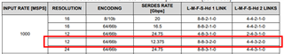
* Encoding : 64b/66b
* Lane late : 12.375 Gbps
* LMFSHd : 44320 (will use 2 lane)
* Input Late : 1.0 Gsps
* Resolution : 12 bits
3. Clock
* Input Clock : 187.5 MHz (Internal PLL input)
* SysRef : 5.20833 MHz (Same as FPGA)
* From LMK04832
4. NCO : 4.25 GHz
5. DAC
* 1 Ch used
* output frequency : 4.25 GHz
* Bandwidth : 1.5 GHz
Thanks.