


Part Number: AFE7950EVM
Other Parts Discussed in Thread: AFE7950, LMK04828, LMK04832
Hi,
Customer wants to use external clock source for jitter cleaner in AFE7950EVM.
Could you guide for this request?

This thread has been locked.
If you have a related question, please click the "Ask a related question" button in the top right corner. The newly created question will be automatically linked to this question.
Part Number: AFE7950EVM
Other Parts Discussed in Thread: AFE7950, LMK04828, LMK04832
Hi,
Customer wants to use external clock source for jitter cleaner in AFE7950EVM.
Could you guide for this request?
Hi David,
Please refer to the "AFE79xx_EVM_External_Clocking_Guide.pptx" in the secure folder under "Users_Guide_and_SW".
Best,
Camilo

Hi Camilo,
Thank you for your guide. However this is not exactly solution for me. What I would like to input the external clock for the jitter cleaner.
And I like to input clock for the AFE7950's reference from the jitter cleaner.
Could you help me how I can do?
Thank you.
Hi Byungsoo,
Sorry for the confusion.
When you say you want to input a clock into the jitter cleaner, I assume you want to use the LMK04828 in dual PLL mode where PLL1 acts as a jitter cleaner instead of giving it a clock to use in distribution mode. If this is correct you must set the following parameters such that the following equation holds:
Fin/R = 122.88/N
Because of the phase detector in the picture below:
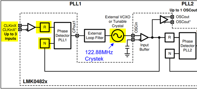
You can change R and N divider values in the AFE79xx GUI by setting the following properties based on your desired Fin.
lmk.head.page.PLL1_Config.Clkin0_1_2_Divider.div_clkin1_lt_13_0_gt_ = R
lmk.head.page.PLL1_Config.N_Divider_PLL1.N_DIV_PLL1_lt_13_0_gt_ = N
And make sure that lmkParams.pllEn = True
Best,
Camilo
Hi Camilo,
Thank you for your reply.
I like to configure the LMK04832 works in internal VCO mode with external reference clock input.
In the EVM board, I would like to change the input clock of the LMK04832 from on board oscillator to external clock.
I don't like to change the other configuration in the EVM board. The external clock is 100 MHz.
So I think some setting values need change because the reference clock is changed.
Could you make me know how I can set it?
Thank you.
Hi Byungsoo,
If your goal is to change the input of the LMK04828 from the on board oscillator to external clock for the PLL2, the EVM is not really designed to support this option. Since the OSCin pins are only connected to the on-board oscillator. If you really want to do something like this there might be three options:
We will provide more guidance depending on the option you pick.
Best,
Camilo
Hi Camilo,
Thank you for your advice.
I like to chose the third of the your advice.
I will wait for your guidance.
Thank you.
Hi Byungsoo,
Ok. To do this, your bring up script must have the following parameters set accordingly:
If there are questions in these parameters please let me know. If you provide your configuration file, your desired input clock to the LMK and your FPGA Ref clock we can help you put it in the script.
Best,
Camilo
Hi Camilo,
I modify a script in latte
Please, check below script.
Thank you.
############## Read me ##############
#External clock is used instead of onboard clock. And LMK04832 is working in distribute mode.
#In HSDC Pro DAC tab, Select AFE79xx_2x2TX_44210; Data Rate = 491.52M
#In HSDC Pro ADC tab, Select AFE79xx_2x2RX_24410; Data Rate = 245.76M ---> To capture 4 RX channels
#In HSDC Pro ADC tab, Select AFE79xx_1x2FB_44210; Data Rate = 491.52M ---> To capture 2 FB channels
sysParams=AFE.systemParams
sysParams.__init__();sysParams.chipVersion=chipVersion
setupParams.skipFpga = 1 # setup FPGA (TSW14J56) using HSDC Pro
############## Top Level ##############
sysParams.FRef = 491.52
sysParams.FadcRx = 2949.12
sysParams.FadcFb = 2949.12
sysParams.Fdac = 2949.12*4
sysParams.externalClockRx=False
sysParams.externalClockTx=False
############## Digital Chain ##############
##### RX #####
sysParams.ddcFactorRx = [12,12,12,12] #DDC decimation factor for RX A, B, C and D
sysParams.rxNco0 = [[5320,5320], #Band0, Band1 for RXA
[5320,5320], #Band0, Band1 for RXB
[5320,5320], #Band0, Band1 for RXC
[5320,5320]] #Band0, Band1 for RXD
##### FB #####
sysParams.ddcFactorFb = [6,6] #DDC decimation factor for FB 1 and 2
sysParams.fbNco0 = [5320,5320] #Band0 for FB1 and FB2
##### TX #####
sysParams.ducFactorTx = [24,24,24,24] #DUC interpolation factor for TX A, B, C and D
sysParams.txNco0 = [[5400,5400], #Band0, Band1 for TXA
[5400,5400], #Band0, Band1 for TXB
[5400,5400], #Band0, Band1 for TXC
[5400,5400]] #Band0, Band1 for TXD
############## JESD ##############
##### ADC-JESD #####
sysParams.jesdSystemMode= [1,1]
#SystemMode 0: 2R1F-FDD ; rx1-rx2-fb -fb
#SystemMode 1: 1R1F-FDD ; rx -rx -fb -fb
#SystemMode 2: 2R-FDD ; rx1-rx1-rx2-rx2
#SystemMode 3: 1R ; rx -rx -rx -rx
#SystemMode 4: 1F ; fb -fb- fb -fb
#SystemMode 5: 1R1F-TDD ; rx/fb-rx/fb-rx/fb-rx/fb
sysParams.jesdTxProtocol= [0,0] # 0 - 8b/10b encoding; 2 - 64b/66b encoding
sysParams.LMFSHdRx = ["24410","24410","24410","24410"]
# The 2nd and 4th are valid only for jesdSystemMode values in (0,2).
# For other modes, select 4 converter modes for 1st and 3rd.
sysParams.LMFSHdFb = ["22210","22210"]
sysParams.rxJesdTxScr = [True,True,True,True]
sysParams.fbJesdTxScr = [True,True]
sysParams.rxJesdTxK = [16,16,16,16]
sysParams.fbJesdTxK = [16,16]
sysParams.jesdTxLaneMux = [0,1,2,3,4,5,6,7] # Enter which lanes you want in each location.
# For example, if you want to exchange the first two lines of each 2T,
# this should be [[1,0,2,3],[5,4,6,7]]
##### DAC-JESD #####
sysParams.jesdRxProtocol= [0,0]
sysParams.LMFSHdTx = ["44210","44210","44210","44210"]
sysParams.jesdRxLaneMux = [0,1,2,3,4,5,6,7] # Enter which lanes you want in each location.
# For example, if you want to exchange the first two lines of each 2R
# this should be [[1,0,2,3],[5,4,6,7]]
sysParams.jesdRxRbd = [4, 4]
sysParams.jesdRxScr = [True,True,True,True]
sysParams.jesdRxK = [16,16,16,16]
##### JESD Common #####
sysParams.jesdABLvdsSync= True
sysParams.jesdCDLvdsSync= True
sysParams.syncLoopBack = True #JESD Sync signal is connected to FPGA
############## GPIO ##############
sysParams.gpioMapping = {
'H8': 'ADC_SYNC0',
'H7': 'ADC_SYNC1',
'N8': 'ADC_SYNC2',
'N7': 'ADC_SYNC3',
'H9': 'DAC_SYNC0',
'G9': 'DAC_SYNC1',
'N9': 'DAC_SYNC2',
'P9': 'DAC_SYNC3',
'P14': 'GLOBAL_PDN',
'K14': 'FBABTDD',
'R6': 'FBCDTDD',
'H15': ['TXATDD','TXBTDD'],
'V5': ['TXCTDD','TXDTDD'],
'E7': ['RXATDD','RXBTDD'],
'R15': ['RXCTDD','RXDTDD']}
############## LMK Params ##############
lmkParams.pllEn = False
lmkParams.inputClk = 491.52 # Valid only when lmkParams.pllEn = False
lmkParams.lmkFrefClk = True
setupParams.fpgaRefClk = 245.76 # Should be equal to LaneRate/40 for TSW14J56
############## Logging ##############
logDumpInst.setFileName(ASTERIX_DIR+DEVICES_DIR+r"\Afe79xxPg1.txt")
logDumpInst.logFormat=0x0 #Modify to 0x1 to save register scequence to log file. Script takes more time to execute.
logDumpInst.rewriteFile=1
logDumpInst.rewriteFileFormat4=1
device.optimizeWrites=0
device.rawWriteLogEn=1
device.delay_time = 0
#-------------------------------------------------------------------------------------------------#
AFE.deviceBringup()
AFE.TOP.overrideTdd(15,3,15) # bit-wise; 4R,2F,4T
Hi Byungsoo,
The changes in the LMK parameters are correct to input an external clock of 491.52MHz.
Best,
Camilo
Hi Camilo,
Today, I test as follow:
1. I connect external 100 MHz clock to J14 on the EVM for LMK_CLK_IN.
2. Execute the High Speed Data Converter Pro
3. Execute the Latte.
4. Set the data rate to 250MHz on the DAC tap of the High Speed Data Converter Pro.
5. Set the others setting to test.
6. Press the send button.
7. I bring up follow the Latte guide.
8. Run the modified python script.
The latte message out likes "SPIA has got control of PLL pages
PLL not locked".
Below added the modified python script. It is tested and the latte output message log.
Please check below the attached python script and the latte output message.
And please make me know what I make mistake.
Thank you.
--------------------- start of python script -------------------
############## Read me ##############
#External clock is used instead of onboard clock. And LMK04832 is working in distribute mode.
#In HSDC Pro DAC tab, Select AFE79xx_2x2TX_24410; Data Rate = 250M
#In HSDC Pro ADC tab, Select AFE79xx_2x2RX_24410; Data Rate = 250M ---> To capture 4 RX channels
#In HSDC Pro ADC tab, Select AFE79xx_1x2FB_24410; Data Rate = 250M ---> To capture 2 FB channels
sysParams=AFE.systemParams
sysParams.__init__();sysParams.chipVersion=chipVersion
setupParams.skipFpga = 1 # setup FPGA (TSW14J56) using HSDC Pro
############## Top Level ##############
sysParams.FRef = 250
sysParams.FadcRx = 6000
sysParams.FadcFb = 6000
sysParams.Fdac = 12000
sysParams.RRFMode = 5 #RRFMode 0: 4T4R2F FDD Mode
#RRFMode 1: 4T4R1F FDD Mode
#RRFMode 2: 4T4R2F FDD Mode Quad Band
#RRFMode 5: 4T4R2F TDD Non-Shared
#RRFMode 6: 4T4R1F TDD Non-Shared
#RRFMode 7: 4T4R2F TDD Shared
#RRFMode 8: 4T4R1F TDD Shared
#RRFMode 10: 2T2R1F TDD AB / 2T2R1F FDD CD
#RRFMode 11: 2T2R1F FDD AB / 2T2R1F TDD CD
sysParams.externalClockRx=False
sysParams.externalClockTx=False
############## Digital Chain ##############
##### RX #####
sysParams.ddcFactorRx = [24,24,24,24] #DDC decimation factor for RX A, B, C and D
sysParams.rxNco0 = [[5400,5400], #Band0, Band1 for RXA
[5400,5400], #Band0, Band1 for RXB
[5400,5400], #Band0, Band1 for RXC
[5400,5400]] #Band0, Band1 for RXD
##### FB #####
sysParams.ddcFactorFb = [24,24] #DDC decimation factor for FB 1 and 2
sysParams.fbNco0 = [5400,5400] #Band0 for FB1 and FB2
##### TX #####
#sysParams.ducFactorTx = [24,24,24,24] #DUC interpolation factor for TX A, B, C and D
sysParams.ducFactorTx = [48,48,48,48] #DUC interpolation factor for TX A, B, C and D
sysParams.txNco0 = [[5400,5400], #Band0, Band1 for TXA
[5400,5400], #Band0, Band1 for TXB
[5400,5400], #Band0, Band1 for TXC
[5400,5400]] #Band0, Band1 for TXD
############## JESD ##############
##### ADC-JESD #####
sysParams.jesdSystemMode= [1,1]
#SystemMode 0: 2R1F-FDD ; rx1-rx2-fb -fb
#SystemMode 1: 1R1F-FDD ; rx -rx -fb -fb
#SystemMode 2: 2R-FDD ; rx1-rx1-rx2-rx2
#SystemMode 3: 1R ; rx -rx -rx -rx
#SystemMode 4: 1F ; fb -fb- fb -fb
#SystemMode 5: 1R1F-TDD ; rx/fb-rx/fb-rx/fb-rx/fb
sysParams.jesdTxProtocol= [0,0] # 0 - 8b/10b encoding; 2 - 64b/66b encoding
sysParams.LMFSHdRx = ["24410","24410","24410","24410"]
# The 2nd and 4th are valid only for jesdSystemMode values in (0,2).
# For other modes, select 4 converter modes for 1st and 3rd.
sysParams.LMFSHdFb = ["24410","24410"]
sysParams.rxJesdTxScr = [True,True,True,True]
sysParams.fbJesdTxScr = [True,True]
sysParams.rxJesdTxK = [16,16,16,16]
sysParams.fbJesdTxK = [16,16]
sysParams.jesdTxLaneMux = [0,1,2,3,4,5,6,7] # Enter which lanes you want in each location.
# For example, if you want to exchange the first two lines of each 2T,
# this should be [[1,0,2,3],[5,4,6,7]]
##### DAC-JESD #####
sysParams.jesdRxProtocol= [0,0]
sysParams.LMFSHdTx = ["24410","24410","24410","24410"]
sysParams.jesdRxLaneMux = [0,1,2,3,4,5,6,7] # Enter which lanes you want in each location.
# For example, if you want to exchange the first two lines of each 2R
# this should be [[1,0,2,3],[5,4,6,7]]
sysParams.jesdRxRbd = [4, 4]
sysParams.jesdRxScr = [True,True,True,True]
sysParams.jesdRxK = [16,16,16,16]
##### JESD Common #####
sysParams.jesdABLvdsSync= True
sysParams.jesdCDLvdsSync= True
sysParams.syncLoopBack = True #JESD Sync signal is connected to FPGA
############## GPIO ##############
sysParams.gpioMapping = {
'H8': 'ADC_SYNC0',
'H7': 'ADC_SYNC1',
'N8': 'ADC_SYNC2',
'N7': 'ADC_SYNC3',
'H9': 'DAC_SYNC0',
'G9': 'DAC_SYNC1',
'N9': 'DAC_SYNC2',
'P9': 'DAC_SYNC3',
'P14': 'GLOBAL_PDN',
'K14': 'FBABTDD',
'R6': 'FBCDTDD',
'H15': ['TXATDD','TXBTDD'],
'V5': ['TXCTDD','TXDTDD'],
'E7': ['RXATDD','RXBTDD'],
'R15': ['RXCTDD','RXDTDD']}
############## LMK Params ##############
lmkParams.pllEn = False
lmkParams.inputClk = 250 # Valid only when lmkParams.pllEn = False
lmkParams.lmkFrefClk = True
setupParams.fpgaRefClk = 250 # Should be equal to LaneRate/40 for TSW14J56
############## Logging ##############
logDumpInst.setFileName(ASTERIX_DIR+DEVICES_DIR+r"\Afe79xxPg1.txt")
logDumpInst.logFormat=0x0 #Modify to 0x1 to save register scequence to log file. Script takes more time to execute.
logDumpInst.rewriteFile=1
logDumpInst.rewriteFileFormat4=1
device.optimizeWrites=0
device.rawWriteLogEn=1
device.delay_time = 0
#-------------------------------------------------------------------------------------------------#
AFE.deviceBringup()
AFE.TOP.overrideTdd(15,3,15) # bit-wise; 4R,2F,4T
--------------------- end of python script -------------------
--------------------- start of latte output message -------------------
#Executing .. AFE7950/bringup/S8_ExternalClk_RX_250M_TX_FB_250M_CENTER_5400MHz.py
#Start Time 2024-02-13 19:50:47.569000
For these rates, 1KHz raster mode is not supported. Changing to 32-bit NCO mode.
The External Sysref Frequency should be an integer factor of: 3.90625MHz
2T2R1F Number: 0
Valid Configuration: True
laneRateRx: 10000.0
laneRateFb: 10000.0
laneRateTx: 10000.0
2T2R1F Number: 1
Valid Configuration: True
laneRateRx: 10000.0
laneRateFb: 10000.0
laneRateTx: 10000.0
Device Initialization for ChipVersion: 1.3
LMK Clock Divider - Device registers reset.
LMK Clock Divider - Device registers reset.
DONOT_OPEN_Atharv_FULL - Device registers reset.
chipType: 0xa
chipId: 0x78
chipVersion: 0x11
SPIA has got control of PLL pages
PLL Pages SPI control relinquished.
Fuse farm load autoload done successful
No autload error
Fuse farm load autoload done successful
No autload error
//Firmware Version = 11000
//PG Version = 1
//Release Date [dd/mm/yy] = 10/7/19
patchSize=11697
//Patch Version = 165
//PG Version = 0
//Release Date [dd/mm/yy] = 27/11/21
SPIA has got control of PLL pages
PLL not locked
#Error: exceptions must be old-style classes or derived from BaseException, not NoneType
# "AFE7950/bringup/S8_ExternalClk_RX_250M_TX_FB_250M_CENTER_5400MHz.py", line 128, in
# File "C:\Users\O21027\Documents\Texas Instruments\Latte\lib\\AFE79xxLibraries\\AFE79xxLibraryPG1p0\resourceFiles\mFuncDecorator.py", line 88, in inDecorator
# a=func(*args,**kwargs)
# File "C:\Users\O21027\Documents\Texas Instruments\Latte\lib\\AFE79xxLibraries\\AFE79xxLibraryPG1p0\mAfeLibrary.py", line 290, in deviceBringup
# self.TOP.configurePll()
# File "C:\Users\O21027\Documents\Texas Instruments\Latte\lib\\AFE79xxLibraries\\AFE79xxLibraryPG1p0\resourceFiles\mFuncDecorator.py", line 88, in inDecorator
# a=func(*args,**kwargs)
# File "C:\Users\O21027\Documents\Texas Instruments\Latte\lib\\AFE79xxLibraries\\AFE79xxLibraryPG1p0\mTopLib.py", line 710, in configurePll
# raise
# TypeError: exceptions must be old-style classes or derived from BaseException, not NoneType
#
#
#Done executing .. AFE7950/bringup/S8_ExternalClk_RX_250M_TX_FB_250M_CENTER_5400MHz.py
#End Time 2024-02-13 19:50:55.036000
#Execution Time = 7.46700000763 s
#================ ERRORS:2, WARNINGS:1 ================#
--------------------- end of latte output message -------------------
Hi Byungsoo,
Just some comments as to why the script did not work.
If you would like, could you give me the following details about your desired mode and I will create a script for you:
Best,
Camilo
Hi Camilo,
Thank you for your reply.
Yes, I use TSW14J57.
Below I would like for setting information. The External clock should be 100 MHz.
Thank you.
Hi Byungsoo,
Just want to clarify something. When you say “The External clock should be 100 MHz” you are referring to the input clock to the LMK correct? Or are you referring to the Fref input to the AFE?
If you are referring to the input of the LMK, the distribution mode of the LMK will not be able to work with 100MHz, because your FPGA refclock is (Lane Rate)/40 for the TSW14J57 and there is no mode with the parameters that you have suggested below to accomplish this.
Therefore, I offer you the following options:
If you would rather go with option 2 please let me know.
Best,
Camilo
Hi, Camilo
Thank you for your reply.
The external clock is connected to J14 SMA connector. As you know J14 SMA connector is connected to CLKIN1 pin of the LMK04832.
As I addressed I like to use the LMK04832 distribute mode with external 100 MHz.
I understood after I read your reply the latte script does not support all of the setting for LMK04832.
I can only set FRef same as lmkParams.inputClk when I use external clock.
So I try to change the script FRef is 100 MHz.
In this case, All of is passed. But the serdes lanes does not receive data from High Speed Data Converter Pro.
I attached the script. Please, Check it and make me know what is wrong.
Thank you.
------------ Start of the script --------------
############## Read me ##############
#External clock is used instead of onboard clock. And LMK04832 is working in distribute mode.
#In HSDC Pro DAC tab, Select AFE79xx_2x2TX_24410; Data Rate = 100M
#In HSDC Pro ADC tab, Select AFE79xx_2x2RX_24410; Data Rate = 100M ---> To capture 4 RX channels
#In HSDC Pro ADC tab, Select AFE79xx_1x2FB_24410; Data Rate = 100M ---> To capture 2 FB channels
sysParams=AFE.systemParams
sysParams.__init__();sysParams.chipVersion=chipVersion
setupParams.skipFpga = 1 # setup FPGA (TSW14J56) using HSDC Pro
############## Top Level ##############
sysParams.FRef = 100
sysParams.FadcRx = 2000
sysParams.FadcFb = 2000
sysParams.Fdac = 4000
sysParams.RRFMode = 5 #RRFMode 0: 4T4R2F FDD Mode
#RRFMode 1: 4T4R1F FDD Mode
#RRFMode 2: 4T4R2F FDD Mode Quad Band
#RRFMode 5: 4T4R2F TDD Non-Shared
#RRFMode 6: 4T4R1F TDD Non-Shared
#RRFMode 7: 4T4R2F TDD Shared
#RRFMode 8: 4T4R1F TDD Shared
#RRFMode 10: 2T2R1F TDD AB / 2T2R1F FDD CD
#RRFMode 11: 2T2R1F FDD AB / 2T2R1F TDD CD
sysParams.externalClockRx=False
sysParams.externalClockTx=False
############## Digital Chain ##############
##### RX #####
sysParams.ddcFactorRx = [20,20,20,20] #DDC decimation factor for RX A, B, C and D
sysParams.rxNco0 = [[5400,5400], #Band0, Band1 for RXA
[5400,5400], #Band0, Band1 for RXB
[5400,5400], #Band0, Band1 for RXC
[5400,5400]] #Band0, Band1 for RXD
##### FB #####
sysParams.ddcFactorFb = [20,20] #DDC decimation factor for FB 1 and 2
sysParams.fbNco0 = [5400,5400] #Band0 for FB1 and FB2
##### TX #####
sysParams.ducFactorTx = [40,40,40,40] #DUC interpolation factor for TX A, B, C and D
sysParams.txNco0 = [[5400,5400], #Band0, Band1 for TXA
[5400,5400], #Band0, Band1 for TXB
[5400,5400], #Band0, Band1 for TXC
[5400,5400]] #Band0, Band1 for TXD
############## JESD ##############
##### ADC-JESD #####
sysParams.jesdSystemMode= [1,1]
#SystemMode 0: 2R1F-FDD ; rx1-rx2-fb -fb
#SystemMode 1: 1R1F-FDD ; rx -rx -fb -fb
#SystemMode 2: 2R-FDD ; rx1-rx1-rx2-rx2
#SystemMode 3: 1R ; rx -rx -rx -rx
#SystemMode 4: 1F ; fb -fb- fb -fb
#SystemMode 5: 1R1F-TDD ; rx/fb-rx/fb-rx/fb-rx/fb
sysParams.jesdTxProtocol= [0,0] # 0 - 8b/10b encoding; 2 - 64b/66b encoding
sysParams.LMFSHdRx = ["24410","24410","24410","24410"]
# The 2nd and 4th are valid only for jesdSystemMode values in (0,2).
# For other modes, select 4 converter modes for 1st and 3rd.
sysParams.LMFSHdFb = ["24410","24410"]
sysParams.rxJesdTxScr = [True,True,True,True]
sysParams.fbJesdTxScr = [True,True]
sysParams.rxJesdTxK = [16,16,16,16]
sysParams.fbJesdTxK = [16,16]
sysParams.jesdTxLaneMux = [0,1,2,3,4,5,6,7] # Enter which lanes you want in each location.
# For example, if you want to exchange the first two lines of each 2T,
# this should be [[1,0,2,3],[5,4,6,7]]
##### DAC-JESD #####
sysParams.jesdRxProtocol= [0,0]
sysParams.LMFSHdTx = ["24410","24410","24410","24410"]
sysParams.jesdRxLaneMux = [0,1,2,3,4,5,6,7] # Enter which lanes you want in each location.
# For example, if you want to exchange the first two lines of each 2R
# this should be [[1,0,2,3],[5,4,6,7]]
sysParams.jesdRxRbd = [4, 4]
sysParams.jesdRxScr = [True,True,True,True]
sysParams.jesdRxK = [16,16,16,16]
##### JESD Common #####
sysParams.jesdABLvdsSync= True
sysParams.jesdCDLvdsSync= True
sysParams.syncLoopBack = True #JESD Sync signal is connected to FPGA
############## GPIO ##############
sysParams.gpioMapping = {
'H8': 'ADC_SYNC0',
'H7': 'ADC_SYNC1',
'N8': 'ADC_SYNC2',
'N7': 'ADC_SYNC3',
'H9': 'DAC_SYNC0',
'G9': 'DAC_SYNC1',
'N9': 'DAC_SYNC2',
'P9': 'DAC_SYNC3',
'P14': 'GLOBAL_PDN',
'K14': 'FBABTDD',
'R6': 'FBCDTDD',
'H15': ['TXATDD','TXBTDD'],
'V5': ['TXCTDD','TXDTDD'],
'E7': ['RXATDD','RXBTDD'],
'R15': ['RXCTDD','RXDTDD']}
############## LMK Params ##############
lmkParams.pllEn = False
lmkParams.inputClk = 100 # Valid only when lmkParams.pllEn = False
#lmkParams.lmkVcoFreq = 3000;
lmkParams.lmkFrefClk = True
setupParams.fpgaRefClk = 100 # Should be equal to LaneRate/40 for TSW14J56
############## Logging ##############
logDumpInst.setFileName(ASTERIX_DIR+DEVICES_DIR+r"\Afe79xxPg1.txt")
logDumpInst.logFormat=0x1 #Modify to 0x1 to save register scequence to log file. Script takes more time to execute.
logDumpInst.rewriteFile=1
logDumpInst.rewriteFileFormat4=1
device.optimizeWrites=0
device.rawWriteLogEn=1
device.delay_time = 0
#-------------------------------------------------------------------------------------------------#
AFE.deviceBringup()
AFE.TOP.overrideTdd(15,3,15) # bit-wise; 4R,2F,4T
------------ End of the script --------------
Hi Byungsoo,
I have made some changes to the script you have posted. The issue was that you just needed some extra writes to set the LMK in bypass mode.
Please try this script with the “AFE79xx_2x2TX_24410” and “AFE79xx_6RX_24410” .ini files in HSDCpro.
############## Read me ##############

#External clock is used instead of onboard clock. And LMK04832 is working in distribute mode with 100MHz input.

#In HSDC Pro DAC tab, Select AFE79xx_2x2TX_24410; Data Rate = 100M

#In HSDC Pro ADC tab, Select AFE79xx_6RX_24410; Data Rate = 100M ---> To capture 4 RX  and 2 FB channels in this order RXA, RXB, FBAB, RXC, RXD, & FBCD

sysParams=AFE.systemParams

sysParams.__init__();sysParams.chipVersion=chipVersion

setupParams.skipFpga = 1 # setup FPGA (TSW14J56) using HSDC Pro

############## Top Level ##############

sysParams.FRef = 100

sysParams.FadcRx = 2400

sysParams.FadcFb = 2400

sysParams.Fdac = 7200

sysParams.RRFMode = 5 #RRFMode 0: 4T4R2F FDD Mode

#RRFMode 1: 4T4R1F FDD Mode

#RRFMode 2: 4T4R2F FDD Mode Quad Band

#RRFMode 5: 4T4R2F TDD Non-Shared

#RRFMode 6: 4T4R1F TDD Non-Shared

#RRFMode 7: 4T4R2F TDD Shared

#RRFMode 8: 4T4R1F TDD Shared

#RRFMode 10: 2T2R1F TDD AB / 2T2R1F FDD CD

#RRFMode 11: 2T2R1F FDD AB / 2T2R1F TDD CD

sysParams.externalClockRx=False

sysParams.externalClockTx=False

############## Digital Chain ##############

##### RX #####

sysParams.ddcFactorRx = [24,24,24,24] #DDC decimation factor for RX A, B, C and D

sysParams.rxNco0 = [[5400,5400], #Band0, Band1 for RXA

[5400,5400], #Band0, Band1 for RXB

[5400,5400], #Band0, Band1 for RXC

[5400,5400]] #Band0, Band1 for RXD

##### FB #####

sysParams.ddcFactorFb = [24,24] #DDC decimation factor for FB 1 and 2

sysParams.fbNco0 = [5400,5400] #Band0 for FB1 and FB2

##### TX #####

sysParams.ducFactorTx = [72]*4 #DUC interpolation factor for TX A, B, C and D

sysParams.txNco0 = [[5400,5400], #Band0, Band1 for TXA

[5400,5400], #Band0, Band1 for TXB

[5400,5400], #Band0, Band1 for TXC

[5400,5400]] #Band0, Band1 for TXD

############## JESD ##############

##### ADC-JESD #####

sysParams.jesdSystemMode= [1,1]

#SystemMode 0: 2R1F-FDD ; rx1-rx2-fb -fb

#SystemMode 1: 1R1F-FDD ; rx -rx -fb -fb

#SystemMode 2: 2R-FDD ; rx1-rx1-rx2-rx2

#SystemMode 3: 1R ; rx -rx -rx -rx

#SystemMode 4: 1F ; fb -fb- fb -fb

#SystemMode 5: 1R1F-TDD ; rx/fb-rx/fb-rx/fb-rx/fb

sysParams.jesdTxProtocol= [0,0] # 0 - 8b/10b encoding; 2 - 64b/66b encoding

sysParams.LMFSHdRx = ["24410","24410","24410","24410"]

# The 2nd and 4th are valid only for jesdSystemMode values in (0,2).

# For other modes, select 4 converter modes for 1st and 3rd.

sysParams.LMFSHdFb = ["24410","24410"]

sysParams.rxJesdTxScr = [True,True,True,True]

sysParams.fbJesdTxScr = [True,True]

sysParams.rxJesdTxK = [16,16,16,16]

sysParams.fbJesdTxK = [16,16]

sysParams.jesdTxLaneMux = [0,1,2,6,4,5,3,7] # Enter which lanes you want in each location.

# For example, if you want to exchange the first two lines of each 2T,

# this should be [[1,0,2,3],[5,4,6,7]]

##### DAC-JESD #####

sysParams.jesdRxProtocol= [0,0]

sysParams.LMFSHdTx = ["24410","24410","24410","24410"]

sysParams.jesdRxLaneMux = [0,1,4,5,2,3,6,7] # Enter which lanes you want in each location.

# For example, if you want to exchange the first two lines of each 2R

# this should be [[1,0,2,3],[5,4,6,7]]

sysParams.jesdRxRbd = [4, 4]

sysParams.jesdRxScr = [True,True,True,True]

sysParams.jesdRxK = [16,16,16,16]

##### JESD Common #####

sysParams.jesdABLvdsSync= True

sysParams.jesdCDLvdsSync= True

sysParams.syncLoopBack = True #JESD Sync signal is connected to FPGA

############## GPIO ##############

sysParams.gpioMapping = {

'H8': 'ADC_SYNC0',

'H7': 'ADC_SYNC1',

'N8': 'ADC_SYNC2',

'N7': 'ADC_SYNC3',

'H9': 'DAC_SYNC0',

'G9': 'DAC_SYNC1',

'N9': 'DAC_SYNC2',

'P9': 'DAC_SYNC3',

'P14': 'GLOBAL_PDN',

'K14': 'FBABTDD',

'R6': 'FBCDTDD',

'H15': ['TXATDD','TXBTDD'],

'V5': ['TXCTDD','TXDTDD'],

'E7': ['RXATDD','RXBTDD'],

'R15': ['RXCTDD','RXDTDD']}

############## LMK Params ##############

lmkParams.pllEn = False

lmkParams.inputClk = 100 # Valid only when lmkParams.pllEn = False

#lmkParams.lmkVcoFreq = 3000;

lmkParams.lmkFrefClk = True

setupParams.fpgaRefClk = 100 # Should be equal to LaneRate/40 for TSW14J56


############## Logging ##############

logDumpInst.setFileName(ASTERIX_DIR+DEVICES_DIR+r"\Afe79xxPg1.txt")

logDumpInst.logFormat=0x1 #Modify to 0x1 to save register scequence to log file. Script takes more time to execute.

logDumpInst.rewriteFile=1

logDumpInst.rewriteFileFormat4=1

device.optimizeWrites=0

device.rawWriteLogEn=1

device.delay_time = 0

##############		Program LMK		##############
setupParams.skipLmk	=	False
AFE.initializeConfig()
lmkParams.sysrefFreq = AFE.systemStatus.sysrefFreq
lmkParams.lmkPulseSysrefMode = False
AFE.LMK.lmkConfig()
AFE.initializeConfig()

lmk.head.page.DCLK0_SDCLK1_controls.Analog_Dig_Delay.dclk_mux_lt_1_0_gt_ = 2
lmk.head.page.DCLK12_SDCLK13_controls.Analog_Dig_Delay.dclk_mux_lt_1_0_gt_ = 2
#-------------------------------------------------------------------------------------------------#

## Initiates AFE79xx Bring-up
setupParams.skipLmk	=	True
## Run init
AFE.deviceBringup()
## RF Enable
AFE.TOP.overrideTdd(15,3,15) # RF Enable Configuration hex(15)=F=0x1111 is all Rx , 1 is single FB=FBab, hex(10)=1010 is only Tx B & Tx D EN3
setupParams.skipLmk	=	False
Your phase noise performance might not be the best in this mode since you are using an Fref lower than the recommended 500MHz for the on-chip PLL.
And if you would like to use the max DAC Fs, we could still provide you with a script that takes the 100MHz external clock into the LMK to lock PLL1, then use the on board Crystal to generate a 3GHz VCO, to then provide the FPGA with a refclock for a mode that can use the max sample rate.
Best,
Camilo
Hi, Camilo
I test you modified latte script.
Below I attached the latte log file.
If you see it, you can understand.
I test on board oscillator with other script likes 491.5M sampling rate.
The script is working and I can see the AFE7950 RF out.
---------- stat of the latte log -----------
#======
#Executing .. AFE7950/bringup/S8_ExternalClk_RX_100M_TX_FB_100M_CENTER_5400MHz_from_TI.py
#Start Time 2024-02-20 15:20:34.063000
For these rates, 1KHz raster mode is not supported. Changing to 32-bit NCO mode.
The External Sysref Frequency should be an integer factor of: 3.125MHz
2T2R1F Number: 0
Valid Configuration: True
laneRateRx: 4000.0
laneRateFb: 4000.0
laneRateTx: 4000.0
2T2R1F Number: 1
Valid Configuration: True
laneRateRx: 4000.0
laneRateFb: 4000.0
laneRateTx: 4000.0
LMK Clock Divider - Device registers reset.
LMK Clock Divider - Device registers reset.
The External Sysref Frequency should be an integer factor of: 3.125MHz
2T2R1F Number: 0
Valid Configuration: True
laneRateRx: 4000.0
laneRateFb: 4000.0
laneRateTx: 4000.0
2T2R1F Number: 1
Valid Configuration: True
laneRateRx: 4000.0
laneRateFb: 4000.0
laneRateTx: 4000.0
The External Sysref Frequency should be an integer factor of: 3.125MHz
2T2R1F Number: 0
Valid Configuration: True
laneRateRx: 4000.0
laneRateFb: 4000.0
laneRateTx: 4000.0
2T2R1F Number: 1
Valid Configuration: True
laneRateRx: 4000.0
laneRateFb: 4000.0
laneRateTx: 4000.0
Device Initialization for ChipVersion: 1.3
DONOT_OPEN_Atharv_FULL - Device registers reset.
chipType: 0xa
chipId: 0x78
chipVersion: 0x11
SPIA has got control of PLL pages
PLL Pages SPI control relinquished.
Fuse farm load autoload done successful
No autload error
Fuse farm load autoload done successful
No autload error
//Firmware Version = 11000
//PG Version = 1
//Release Date [dd/mm/yy] = 10/7/19
patchSize=11697
//Patch Version = 165
//PG Version = 0
//Release Date [dd/mm/yy] = 27/11/21
SPIA has got control of PLL pages
PLL Locked
PLL Pages SPI control relinquished.
SPIA has got control of PLL pages
PLL Pages SPI control relinquished.
SPIA has got control of PLL pages
PLL Pages SPI control relinquished.
SPIA has got control of PLL pages
PLL Pages SPI control relinquished.
Sysref Read as expected
###########Device DAC JESD-RX 0 Link Status###########
Serdes-FIFO error for lane 0: 1
Serdes-FIFO error for lane 1: 1
Comma Align Lock Lane0: False; Please check if the transmitter is sending data and eye is good.
Comma Align Lock Lane1: False; Please check if the transmitter is sending data and eye is good.
CS State TX0: 0b00000000 . It is expected to be 0b00001010
FS State TX0: 0b00000000 . It is expected to be 0b00000101
Couldn't get the link up for device RX: 0; Alarms: 0x3000
###################################
###########Device DAC JESD-RX 1 Link Status###########
Serdes-FIFO error for lane 0: 1
Serdes-FIFO error for lane 1: 1
Comma Align Lock Lane0: False; Please check if the transmitter is sending data and eye is good.
Comma Align Lock Lane1: False; Please check if the transmitter is sending data and eye is good.
CS State TX0: 0b00000000 . It is expected to be 0b00001010
FS State TX0: 0b00000000 . It is expected to be 0b00000101
Couldn't get the link up for device RX: 1; Alarms: 0x3000
###################################
#Done executing .. AFE7950/bringup/S8_ExternalClk_RX_100M_TX_FB_100M_CENTER_5400MHz_from_TI.py
#End Time 2024-02-20 15:21:32.608000
#Execution Time = 58.5450000763 s
#================ ERRORS:10, WARNINGS:1 ================#
---------- end of the latte log -----------
Thank you.
Hi Byungsoo,
Just to clarify, did the script end up working for you? The reason I ask is because I see that you said "The script is working and I can see the AFE7950 RF out." but in the log you posted it says that the JESD link is not up.
If there is an issue, two things to try would be to make sure the J57 FPGA is sending TX data before running the AFE bringup and to run AFE.adcDacSync(1) after bringup to check the link status.
Best,
Camilo
Hi, Camilo
When I see the RF out, the used script and the test configuration is different.
As I mentioned, when I test the different script, the LMK clock source is on board oscillator.
Why I test like this, I like to check the board working or not. The result mean the board is working.
The testing has another meaning the testing sequence has no problem.
Such as High speed data converter pro is sending TX data before running the AFE bringup.
I attached the log after command the AFE.adcDacSync(1) in the Command Line window of the Latte.
I command it after AFE bringup.
Thank you.
--------------- start of the log -----------------
SPIA has got control of PLL pages
PLL Pages SPI control relinquished.
###########Device DAC JESD-RX 0 Link Status###########
Serdes-FIFO error for lane 0: 1
Serdes-FIFO error for lane 1: 1
Comma Align Lock Lane0: False; Please check if the transmitter is sending data and eye is good.
Comma Align Lock Lane1: False; Please check if the transmitter is sending data and eye is good.
CS State TX0: 0b00000000 . It is expected to be 0b00001010
FS State TX0: 0b00000000 . It is expected to be 0b00000101
Couldn't get the link up for device RX: 0; Alarms: 0x3000
###################################
###########Device DAC JESD-RX 1 Link Status###########
Serdes-FIFO error for lane 0: 1
Serdes-FIFO error for lane 1: 1
Comma Align Lock Lane0: False; Please check if the transmitter is sending data and eye is good.
Comma Align Lock Lane1: False; Please check if the transmitter is sending data and eye is good.
CS State TX0: 0b00000000 . It is expected to be 0b00001010
FS State TX0: 0b00000000 . It is expected to be 0b00000101
Couldn't get the link up for device RX: 1; Alarms: 0x3000
###################################
#======
--------------- end of the log -----------------
Hi Byungsoo,
Could you please confirm that you are using the latest version of the AFE79xx Latte GUI that is posted in the secure folder?
After doing the AFE bringup, is LED D2 in the TSW14J57 blinking?
Are you sure you are using the “AFE79xx_2x2TX_24410” and “AFE79xx_6RX_24410” .ini files in HSDCpro?
Best,
Camilo
Hi, Camilo
Thank you for your reply.
Today, I see the RF Out. I don't know what is different.
Today I select AFE79xx_2x2TX_24410.
Yesterday and before. I selected the AFE79xx_2x2TX_24410-B. Even I select again the AFE79xx_2x2TX_24410-B today. I can see the RF Out.
I used the Latte version is 5.4. The LED D2 on the TSW14J57 is blinking.
It is working.
Thank you. Calmilo.
Hi Byungsoo,
When using the TSW14J57 you must first use the "AFE79xx_2x2TX_24410" file and after you have used the "AFE79xx_6RX_24410" file and see that the output is stable you can use the files with the "-B" at the end.
For more information please refer to the "AFE79xxEVM_TSW14J57_BringupGuides.zip" in the secure folder.
Best,
Camilo