


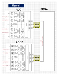
Part Number: AFE7906
The FPGA and ADC1 (AFE7906) and ADC2 (AFE7906) are connected.
I would like to configure the MUX as shown in Figure 1.
Output ADC input data of ADC1_1RX to ADC1_Lane1(3stx)
Output ADC input data of ADC1_2RX to ADC1_Lane2(4stx)
Output ADC input data of ADC1_3RX to ADC1_Lane3(5stx)
Output ADC input data of ADC1_4RX to ADC1_Lane4(6stx)
Output ADC input data of ADC2_1RX to ADC2_Lane1(3stx)
Output ADC input data of ADC2_2RX to ADC2_Lane2(4stx)
Output ADC input data of ADC2_3RX to ADC2_Lane3(5stx)
Output ADC input data of ADC2_4RX to ADC2_Lane4(6stx)
Which MUX configuration is better, figure2 or figure3?
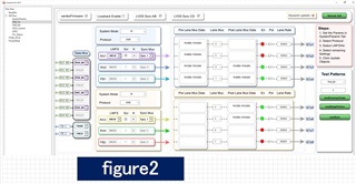
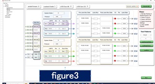
For figure2 and figure3, when setting RAMP test to ADC1 and ADC2 in Latte
AFE.JESD.ADCJESD[0].adcRampTestPattern(0,1,0) #chNo, En, RampInc: RxA
AFE.JESD.ADCJESD[0].adcRampTestPattern(1,1,1) #chNo, En, RampInc: RxB
AFE.JESD.ADCJESD[1].adcRampTestPattern(0,1,2) #chNo, En, RampInc: RxC
AFE.JESD.ADCJESD[1].adcRampTestPattern(1,1,3) #chNo, En, RampInc: RxD
Does the output look like the one below?
ADC1_Lane1 RampInc 1
ADC1_Lane2 RampInc 2
ADC1_Lane3 RampInc 3
ADC1_Lane4 RampInc 4
ADC2_Lane1 RampInc 1
ADC2_Lane2 RampInc 2
ADC2_Lane3 RampInc 3
ADC2_Lane4 RampInc 4
