This thread has been locked.

If you have a related question, please click the "Ask a related question" button in the top right corner. The newly created question will be automatically linked to this question.

AFE7900EVM: Assistance Needed for FPGA Pin Selection for SPI Communication between ZCU102 and AFE7900/LMK

Part Number: AFE7900EVM
Other Parts Discussed in Thread: AFE7900, AFE7950EVM, , AFE7950

Tool/software:

Hello everyone,

I am currently working on a project using the ZCU102 board in conjunction with the AFE7900. My goal is to directly write SPI commands from the FPGA to both the AFE7900 and LMK chips, bypassing the FTDI.

I have been following the instructions provided in the sbau412a document, and have successfully created a block design in Vivado. However, I'm facing some confusion when it comes to selecting the correct FPGA pin numbers for the output of the block diagram.

Specific Issues:

In Section 10 of the document, it discusses AFE79xxEVM Board Modifications. It mentions the SPI lines for the LMK’s chip select, which is associated with pin D26 of the FMC connector. The schematic refers to D26 as SPIASDO_FMC.

Should I use the D26 pin for the LMK’s chip select, or is this pin misidentified in the documentation? How should I correctly map the SPI lines (MOSI, MISO, SCLK, CS) for both the AFE7900 and LMK to FPGA pins?

Section 11 - AXI GPIO Configuration: The document also talks about configuring the AXI GPIO, but I am unclear on how to properly map these to the physical I/O pins of the FPGA for SPI communication.

  • Hi Bala,

    In regards to the LMK chip select, in the guide we mention connecting it to pin D26 of the FMC because by default this pin on the FMC is not connected to the SPIASDO signal since resistor R9 is not installed by default. Therefore this is a unconnected pin on the FMC and we are repurposing it to be used as the LMK chip select.

    Please follow section 10 'AFE79xxEVM Board Modifications' in the app note for connecting the SPI lines correctly for both AFE and LMK. These exact changes were made on our boards and were verified with a reference design. 

    For the AXI GPIO signals, you can add the GPIO module into your block design and connect the outputs of this module to open pins on the FMC connector or other FPGA pins in the block design by making them an external signal. 

    Regards,

    David Chaparro 

  • Hi David,

    Can I get any reference block design for the SPI bringup. I am using vivado 2020.1 or if you have any constraint file for this block design, can you share it?

    I have made a design and build the project in vitis 2020.1. I tried to print some debug messages using xil_print() function, but I didn't get any logs on the console. To verify my design and FPGA pin selections, I need any reference files if you have.

    Regards,

    Bala

  • Hi Bala,

    Please see the constraints file below for the AFE7950EVM+ZCU102.

    4812.hpc0_constraints.xdc

    Regards,

    David Chaparro

  • Hi David,

    I am working with AFE7900EVM + ZCU102. I think I can't use this constraint file. I need a constaint file for AFE7900. 

    Looking for your help.

    Regards,

    Bala

  • Hi Bala,

    The FMC connections on the AFE7900 and AFE7950 EVMs are the same, so the same pin constraints will work.

    Regards,

    David Chaparro 

  • Hi David,

    I checked the pins that you have mentioned in the constraint file. I searched for the pins in my zcu102 user guide. I didn't found any pins connected to the HPC0 FMC connectors.

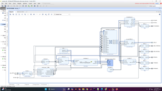
    Do you have any document to create a block design for this becasue I am not sure about the design I created. I have attached the snapshot of my design.

    Regards, 

    Bala

  • Hi Bala,

    The document linked below goes over each step in creating the reference design and in Figure 4-1 shows what the block design should look like. Your design looks to be what is expected. 

    https://www.ti.com/lit/ug/sbau412a/sbau412a.pdf 

    In regards to the constraints, there was an issue with the other constraints and i have updated them below.

    hpc0_constraints.xdc

    Regards,

    David Chaparro 

  • Hi David,

    I checked the constraint files fpga pin number in the zcu102 datasheet, still some of the pins are not matching. The sys_clock pin in zcu102 is AL8 but you chose Y4 and Y2. The uart pins in my zcu102 is E13 and F13 but you chose v4 and v3. I didn't get clarified for this pins. 

    I created the block design using the sbau412a document. But while debugging I am getting the junk characters. I checked the baud rate and clock frequency of my uart16550. Baud rate is 9600 and uart clock frequency is 100 MHz. I don't know why I am getting the junk characters.

    Regards,

    Bala

  • Hi Bala, 

    I believe there is confusion on the clocks and signals being used in the reference design constraints file. The sys_clk_p in the constraints file is the JESD core clock that is used get samples from lane data for the ADC and combine samples into lane data for the DAC. This clock should be provided by the LMK on the AFE EVM. The SYSREF also must come from the same clock source which is why it also comes for the AFE EVM through the FMC connector. The Y4 and Y2 pins for these two are correct and used on all of our ZCU102 reference designs. For more information on these two signals I would recommend referencing sections 6.4 and 6.6 of the TI204c-IP User's Guide. 


    The clocks to the microblaze and spi modules use an onboard clock, pin AL8, and Vivado auto assigns the pins when the clocking wizard selects 'user_si570_sysclk' from the ZCU102 board clock sources. 

    For the UART we are not using V4 and V3. V4 and V3 are used for the AFEs ADC and DAC sync pins which are required when operating in 8b10b encoding. If you are using 64b66b encoding then you do not need the sync signals and they can be commented out in the constraints file. The ZCU102 has defined UART pins so when Vivado  auto routes the uart16550 block it will auto assign the 'uart2_pl' bus to the correct pins, E13 and F13. 

    Regards,

    David Chaparro 

  • Hi David,

    Thanks for your assistance.

    I have tested the design by connecting the spi lines to the gpio pins and I verified the output with logic analyser. I am getting the same commands and I am also getting the debug logs of configuration.

    So now I have to change the SPI lines to FMC connector. Based on the sbau412a document I am clear for selecting the spi lines of AFE. But I am bit confused on selecting the CS line for LMK. 

    I need 3 pins for LMK SDO(MOSI), SEN(CS) and SCK(CLK). But in this document they have mentioned about the SDIO(MISO). And then for LMK_CS they talk about R9 but the R9 is connected to the SPIASDO_FMC which is the SDO of AFE SPI line. Are they mentioned correct in the document?

    I just need this part to complete the setup. I need your assistance for selecting pins for LMK SPI lines.

    Regards,

    Bala

  • Hi Bala,

    The document is correct. For this design we are sharing the SCLK and MISO between AFE and LMK. For the LMK_CS we are connecting a wire from the AFE to an open pad of R9. By default R9 is not populated so there is no issue with connecting to the open pad of R9 that is connected to the FMC connector.

    Regards,

    David Chaparro 

  • Hi David,

    In the c code there will be some functions that will sent the signals to AFE like restting AFE, enable JESD IP, enable JESD TXIP. I think that signals should be sent to the AFE7900. In the document, there is no clarification on where to connect these outputs(FPGA pin number on FMC). 

    Can I know about these? I have searched for this but I didn't get any info for this. The bits they toggling in the function  are JESD RSTn, JESD TXRST, RSTn. 

    I need assistance for this. 

    Regards,

    Bala

  • Hi Bala, 

    In the C code we have functions to control the AFE reset and JESD resets. In order for the microblaze to control the signals the following should be done.

    1. For the AFE reset there is one board modification needed, R94 should be removed and R93 should be installed. 
      1. On the ZCU102 side you should connect the AFE reset signal to pin T6 on the FPGA (FMC pin H32)
    2. The JESD reset signals are only for the JESD IP and do not need to go to the AFE. Instead you can connect the signals, outputs of the GPIO module, and connect them to the JESD IP's master_reset_n, tx_sync_reset, and rx_sync_reset signals, which are currently connected to the VIOs. You can remove the connection from the VIO.

    Regards,

    David Chaparro 

  • Hi David,

    Thanks for the help.

    So now I have two pins left which are JESD_RSTn and JESD_TXRST. Where can I connect these to in JESD IP? I didn't find any ports to connect these two pins.

    And Did you mentioned this JESDIP or TI_IP204?

    Regards,

    Bala

  • Hi Bala,

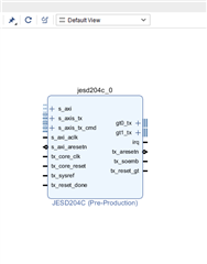
    I was referring to the TI JESD204c IP. Are you using one of our provided reference designs? I assumed you were already using one of our reference designs which has the reset signals that I previously mentioned. In order to bringup a successful JESD link the JESD IP is required on the FPGA side otherwise you would get JESD errors when bringing up the AFE.

    Regards,

    David Chaparro 

  • Hi David,

    Thanks for your assistance. The design was working fine.

    Regards,

    Bala