Part Number: AFE7950EVM
Other Parts Discussed in Thread: AFE7950
Tool/software:
Good morning.
Our team is trying to configure the AFE7950EVM board connected to TSW14J58 board with Latte software. We want to configure the ADCs in a way where the ADCs decimation values are 3 for one block and 2 for the other block, as options indicated into the datasheet.
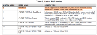
The system mode chosen is rrfmode 0, where Rx,Tx and Fb are at FDD mode
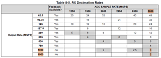
However, once the configuration is compiled by Latte, the error message "Current RX DDC Factor setting not supported in FDD Mode" is returned. Looking around the python code of Latte, this limitation is hardcoded at software which says that for an Output Rate of 1000 and 1500 with ADC sample rate of 3000, 2500 or 2000 the FFD mode is not available.
Which is the reason? Is there a way to get similar behaviour with other configuration?
The expected behaviour is as follow: 4Rx and 4Tx no feedback, 64b/66b, single band at 3600MHz, two ADC with output rate of 1000Msps and 2 ADC with 1500 Msps, 2 DAC with input rate of 1000Msps and other 2 with 1500Msps. To avoid alliasing at DACs, the valid DAC sample rates in our design would be 6000 and 12000 Msps.
Current bringup file used into Latte is as follow:
##############		Read me			##############
#In HSDC Pro DAC tab, Select AFE79xx_2x2TX_44210; Data Rate = 491.52M
#In HSDC Pro ADC tab, Select AFE79xx_2x2RX_24410; Data Rate = 245.76M ---> To capture 4 RX channels
#In HSDC Pro ADC tab, Select AFE79xx_1x2FB_44210; Data Rate = 491.52M ---> To capture 2 FB channels

sysParams=AFE.systemParams
sysParams.__init__();sysParams.chipVersion=chipVersion

setupParams.skipFpga = 0 # setup FPGA (TSW14J58)

##############		Top Level			##############
sysParams.FRef			= 491.52     # Recommended 2949.12/6 (interno o externo, ahora es interno)
sysParams.FadcRx		= 2949.12    # Dependen de si el reloj es interno o externo (ahora mismo es interno )
sysParams.FadcFb		= 2949.12    # Dependen de si el reloj es interno o externo (ahora mismo es interno )
sysParams.Fdac			= 2949.12*2  # Dependen de si el reloj es interno o externo (ahora mismo es interno )
sysParams.externalClockRx=False      # Dependen de si el reloj es interno o externo (ahora mismo es interno )
sysParams.externalClockTx=False      # Dependen de si el reloj es interno o externo (ahora mismo es interno)

##############		Digital Chain		##############

sysParams.RRFMode		= 0					# FDD Mode. This is a typical FDD mode with 4TX, 4RX chains and 2 FB chains,
                                            # where all RX and FB chains have independent ADCs

sysParams.ncoFreqMode = "FCW"

# Its possible to configur number of NCO by band

		#####	RX	#####
sysParams.ddcFactorRx	=	[3,3,2,2]			    #DDC decimation factor for RX A, B, C and D
sysParams.numBandsRx    =   [0,0,0,0]   # Single band
# Rx A B BW 500MHz -> Relacion 1000/3000 Msps - 3
# Rx B C BW 1GHz   -> Relacion 1500/3000 Msps - 2
sysParams.rxNco0		= 	[[3600,3600],			#Band0, Band1 for RXA (media entre 3.3-3.9 GHz)
							[3600,3600],        	#Band0, Band1 for RXB (media entre 3.3-3.9 GHz)
							[3600,3600],        	#Band0, Band1 for RXC
							[3600,3600]]        	#Band0, Band1 for RXD

		#####	FB	#####
sysParams.fbEnable		=	[False,False]
sysParams.ddcFactorFb	=	[3,3]					#DDC decimation factor for FB 1 and 2
sysParams.fbNco0		= 	[3600,3600]				#Band0 for FB1 and FB2

		#####	TX	#####
sysParams.ducFactorTx	=	[6,6,4,4]			#DUC interpolation factor for TX A, B, C and D
sysParams.numBandsTx    =   [0,0,0,0]   # Single band
sysParams.txNco0		= 	[[4450,3600],			#Band0, Band1 for TXA
							[4450,3600],        	#Band0, Band1 for TXB
							[4450,3600],        	#Band0, Band1 for TXC
							[4450,3600]]        	#Band0, Band1 for TXD


##############		JESD		##############

		#####	ADC-JESD	#####
sysParams.jesdSystemMode= [3,3] # case where, FB is not needed and only both channels of the RX
                                # are to be treated as a single JESD mapper

sysParams.jesdTxProtocol= [2,2]						# 0 - 8b/10b encoding; 2 - 64b/66b encoding
sysParams.LMFSHdRx		= ["44210","44210","44210","44210"]

sysParams.LMFSHdFb		= ["22210","22210"]

sysParams.rxJesdTxScr	= [False,False,False,False]
sysParams.fbJesdTxScr	= [False,False]

sysParams.rxJesdTxK		= [1,1,1,1] # Multiblock para 64b - 1
sysParams.fbJesdTxK		= [1,1]     # Multiblock para 64b - 1

sysParams.jesdTxLaneMux	= [0,1,2,3,4,5,6,7]			# Enter which lanes you want in each location.
													# For example, if you want to exchange the first two lines of each 2T,
													#		this should be [[1,0,2,3],[5,4,6,7]]

		#####	DAC-JESD	#####
sysParams.jesdRxProtocol= [2,2]
sysParams.LMFSHdTx		= ["44210","44210","44210","44210"]

sysParams.jesdRxLaneMux	= [0,1,2,3,4,5,6,7]			# Enter which lanes you want in each location.
													# For example, if you want to exchange the first two lines of each 2R
													#		this should be [[1,0,2,3],[5,4,6,7]]
sysParams.jesdRxRbd		= [4, 4]
sysParams.jesdRxScr		= [False,False,False,False]
sysParams.jesdRxK		= [1,1,1,1] # Multiblock para 64b - 1

		#####	JESD Common	#####

sysParams.jesdABLvdsSync= True
sysParams.jesdCDLvdsSync= True
sysParams.syncLoopBack	= False	#JESD Sync signal is connected to FPGA

##############		GPIO		##############
sysParams.gpioMapping	= {
						'H8': 'ADC_SYNC0',
						'H7': 'ADC_SYNC1',
						'N8': 'ADC_SYNC2',
						'N7': 'ADC_SYNC3',
						'H9': 'DAC_SYNC0',
						'G9': 'DAC_SYNC1',
						'N9': 'DAC_SYNC2',
						'P9': 'DAC_SYNC3',
						'P14': 'GLOBAL_PDN',
						'K14': 'FBABTDD',
						'R6': 'FBCDTDD',
						'H15': ['TXATDD','TXBTDD'],
						'V5': ['TXCTDD','TXDTDD'],
						'E7': ['RXATDD','RXBTDD'],
						'R15': ['RXCTDD','RXDTDD']}

##############		LMK Params		##############
lmkParams.pllEn			= True
lmkParams.inputClk		= 983.04 # Valid only when lmkParams.pllEn = False
lmkParams.lmkFrefClk	= True
setupParams.fpgaRefClk	= 245.76 # 2949.12/12

##############		Logging		##############
logDumpInst.setFileName(ASTERIX_DIR+DEVICES_DIR+r"\Afe79xxPg1.txt")
logDumpInst.logFormat=0x1 #Modify to 0x1 to save register scequence to log file. Script takes more time to execute.
logDumpInst.rewriteFile=1
logDumpInst.rewriteFileFormat4=1
device.optimizeWrites=0
device.rawWriteLogEn=1

device.delay_time = 0
#-------------------------------------------------------------------------------------------------#
AFE.deviceBringup()

AFE.TOP.overrideTdd(15,0,15)	# bit-wise; 4R,0F,4T
Any help would appreciate.
Thank you for your time.
Jose

