


Other Parts Discussed in Thread: AFE7906, LMK04828,
Tool/software:
Hello Team,
CASE 1: As we are working on custom board using AFE7906 ADC, First we have implemented the below configuration to test the ADC.
-- LMK04828 input frequency = 61.44 MHz, 7 dBm, which use 122.88 MHz crystal to generate Fs=2949.12 MHz and FPGA clock freq = 184.32 MHz (7372.8 MHz/40).
-- ADC is configured for lanerate=7372.8 MHz & Fs=2949.12 MHz.
Case 1 is working on custom board.
CASE 2: Now we are trying to change the configuration as per project requirement.
-- LMK04828 input frequency = 100 MHz, 7 dBm. which has to generate Fs=2600 MHz and FPGA clock freq = 195 MHz (7800 MHz/40).
-- ADC configuration, lanerate=7800 MHz, Fs=2600 MHz.
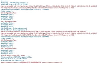
For CASE 2 we are getting errors in python script,both script and errors are attached for reference.
Setup : To generate the registers for custom board AFE7906 ADC using AFE7900EVM Board:
Clock of 100 MHz as input to LMK at J14 connector in AFE7900EVM board.
sysParams							=AFE.systemParams
setupParams.skipFpga 				= 1
setupParams.fpgaRefClk 				= 260
AFE.systemStatus.loadTrims			= 1

sysParams.FRef                    	= 2600 #433.33 #491.52
sysParams.FadcRx                  	= 2600 #2949.12
sysParams.FadcFb				  	= 2600 #2949.12
sysParams.Fdac                    	= 2600 # 8847.36
sysParams.externalClockRx           = False   # enabled on 20-08-2024
sysParams.externalClockTx           = False   # enabled on 20-08-2024

sysParams.rxEnable                  =[True,False,True,False]
sysParams.fbEnable                  =[False,False]
sysParams.txEnable                  =[False,False,False,False]
sysParams.enableDacInterleavedMode	= False 					#DAC interleave mode to save power consumption. Fs/2 - Fin spur occurs

sysParams.modeTdd 					= 0
										# 0- Single TDD Pin for all Channels
										# 1- Separate Control for 2T/2R/1F
										# 2- Separate Control for 1T/1R/1F

sysParams.topLevelSystemMode		= 'StaticTDDMode'
sysParams.RRFMode 					= 0   #4T4R2F FDD mode
sysParams.jesdSystemMode			= [3,3]
										#SystemMode 0:	2R1F-FDD						; rx1-rx2-fb-fb
										#SystemMode 1:	1R1F-FDD						; rx1-rx1-fb-fb
										#SystemMode 2:	2R-FDD							; rx1-rx1-rx2-rx2
										#SystemMode 3:	1R								; rx1-rx1-rx1-rx1
										#SystemMode 4:	1F								; fb-fb-fb-fb
										#SystemMode 5:	1R1F-TDD						; rx1/fb-rx1/fb-rx1/fb-rx1/fb
										#SystemMode 8:	1R1F-TDD 1R-FDD	(FB-2Lanes)(RX1 RX2 interchanged)		; rx2/fb-rx2/fb-rx1-rx1


sysParams.jesdLoopbackEn			= 0 #Make it 1 to Enable the JESDTX to JESDRX internal loopback
sysParams.LMFSHdRx                	=['12610', '12610', '12610', '12610']
sysParams.LMFSHdFb                	= ["12610","12610"]
sysParams.LMFSHdTx                	= ["24410","24410","24410","24410"]
sysParams.jesdTxProtocol            = [0,0]
sysParams.jesdRxProtocol            = [0,0]
sysParams.serdesFirmware			= True 		# If you want to lead any firmware, please speify the path here. Otherwise it will not write any firmware
sysParams.jesdTxLaneMux				= [0,1,2,3,4,5,6,7]
												# Enter which lanes you want in each location.
												# Note that across 2T Mux is not possible in 0.5.
												# For example, if you want to exchange the first two lines of each 2T, this should be [[1,0,2,3],[5,4,6,7]]
sysParams.jesdRxLaneMux				= [0,1,2,3,4,5,6,7]
												# Enter which lanes you want in each location.
												# Note that across 2R Mux is not possible in 0.5.
												# For example, if you want to exchange the first two lines of each 2R, this should be [[1,0,2,3],[5,4,6,7]]
sysParams.txDataMux					= [2,3,0,1,4,5,6,7]
sysParams.jesdRxRbd					= [4, 4]

sysParams.rxJesdTxScr				= [False,False,False,False]
sysParams.fbJesdTxScr				= [False,False]
sysParams.jesdRxScr					= [False,False,False,False]
sysParams.serdesTxLanePolarity		= [False,False,False,False,False,False,False,False]

sysParams.rxJesdTxK					= [32,32,32,32]
sysParams.fbJesdTxK					= [32,32]
sysParams.jesdRxK					= [32,32,32,32]

sysParams.ncoFreqMode 				= "FCW"

# NCO 0 SETTINGS

sysParams.txNco0					= 	[[2890,2890],		#Band0, Band1 for TxA for NCO0
										[2890,2890],        #Band0, Band1 for TxB for NCO0
										[2890,2890],        #Band0, Band1 for TxC for NCO0
										[2890,2890]]        #Band0, Band1 for TxD for NCO0

sysParams.rxNco0					= 	[[2890,2890],		#Band0, Band1 for RxA for NCO0
										[2890,2890],        #Band0, Band1 for RxB for NCO0
										[2890,2890],        #Band0, Band1 for RxC for NCO0
										[2890,2890]]        #Band0, Band1 for RxD for NCO0

sysParams.fbNco0					= 	[2890,2890]			#FBA, FBC for NCO0


sysParams.numBandsRx				= [0]*4					# 0 for single, 1 for dual
sysParams.numBandsFb				= [0,0]
sysParams.numBandsTx				= [0,0,0,0]

sysParams.ddcFactorRx             	= [20,20,20,20]			# DDC decimation factor for RX A, B, C and D
sysParams.ddcFactorFb             	= [20,20]
sysParams.ducFactorTx             	= [36,36,36,36]


## The following parameters sets up the LMK04828 clocking schemes
lmkParams.pllEn						=	False
lmkParams.inputClk					=	100
lmkParams.sysrefFreq				=	4.0625
lmkParams.lmkFrefClk				=	True

## The following parameters sets up the register and macro dumps
logDumpInst.setFileName(ASTERIX_DIR+DEVICES_DIR+r"\Afe79xxPg1_fin_12.txt")
logDumpInst.logFormat				= 0x21 #0x01
logDumpInst.rewriteFile				= 1
logDumpInst.rewriteFileFormat4		= 1
device.optimizeWrites				= 0
device.rawWriteLogEn				= 1

## The following parameters sets up the SYNCIN and SYNCOUT to interface with the TSW14J57
sysParams.jesdABLvdsSync			= False
sysParams.jesdCDLvdsSync			= False
sysParams.rxJesdTxSyncMux			= [0,0,0,0]
sysParams.fbJesdTxSyncMux			= [0,0]
sysParams.jesdRxSyncMux				= [0,0,0,0]		#[0,0,1,1]
sysParams.syncLoopBack				= True
sysParams.serdesFirmware			= True


## The following parameters sets up the GPIOs
sysParams.gpioMapping={
		'H8': 'ADC_SYNC0',
		'H7': 'DAC_SYNC1',
		'N8': 'ADC_SYNC2',
		'N7': 'ADC_SYNC3',
		'H9': 'DAC_SYNC0',
		'G9': 'ADC_SYNC1',
		'N9': 'DAC_SYNC2',
		'P9': 'DAC_SYNC3',
		'P14': 'GLOBAL_PDN',
		'K14': 'FBABTDD',
		'R6': 'FBCDTDD',
		'H15': ['TXATDD','TXBTDD'],
		'V5': ['TXCTDD','TXDTDD'],
		'E7': ['RXATDD','RXBTDD'],
		'R15': ['RXCTDD','RXDTDD'],
		#'G16': ['RX_NCOSEL_0','RX_NCOSEL_1'],# ADDED ON 02-11-23
		#'L14': ['TX_NCOSEL_0','TX_NCOSEL_2'],# ADDED ON 02-11-23
#		'H11': ['TX_NCOSEL_0','TX_NCOSEL_2'],
#		'H16': ['FB_NCOSEL_0','FB_NCOSEL_2']
	}


## Initiates LMK04828 and AFE79xx Bring-up
setupParams.skipLmk	=	False

AFE.initializeConfig()
lmkParams.sysrefFreq = AFE.systemStatus.sysrefFreq
lmkParams.lmkPulseSysrefMode = False
AFE.LMK.lmkConfig()
## Initiates AFE79xx Bring-up
setupParams.skipLmk	=	True
AFE.deviceBringup()

AFE.TOP.overrideTdd(15,0,15)

### ADC Ramp Out
for i in range(3):
	AFE.JESD.ADCJESD[0].adcRampTestPattern(i,0,1)
	AFE.JESD.ADCJESD[1].adcRampTestPattern(i,0,1)


for i in range(4):
	AFE.DSA.setRxDsa(i,10)


AFE.adcDacSync(0)
Kindly help us to resolve the issue asap.
Regards,
Malwinder
