Tool/software:
Hi team,
This is FAE Jayden, my customer is using ADS58J63 in their wireless infrastructure product. Here're some questions from my customer:
1. How to configure the device to select which mode? Is the mode selection achieved by configuring the register through SPI communication?
2. Can I switch between normal mode and burst mode while the device is running? How to enable or switch to burst mode? How to trigger high-resolution sampling after switching to burst mode?
3. Is the only difference between burst mode and normal mode in resolution? Will the frequency of the sampled digital signal transmitted to the FPGA change?
4. In the typical circuit diagram in datasheet, CLKINP/CLKINM and SYSREFP/SYSREFM are both clocked by a clock generator. What is the general setting frequency of this external clock? Is there a recommended device for this clock? Can it be implemented by programming a fixed-frequency flip level using an IO port of the FPGA? What are the frequencies of CLKINP/CLKINM and SYSREFP/SYSREFM?
5. Is the 1.15V of IOVDD a built-in power supply of the device, or does it require an external 1.15V power supply? Can the 1.9V DVDD and AVDD be powered together?
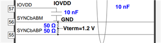
6. Is SYNCbABP/SYNCbABM an IO port connected to the FPGA? How should this IO be configured? What do the 100 ohm and Vterm=1.2V marked in the typical circuit mean? What is the specific link from SYNCbABP/SYNCbABM to FPGA?
Many thanks.
Brs
Jayden