This thread has been locked.

If you have a related question, please click the "Ask a related question" button in the top right corner. The newly created question will be automatically linked to this question.

AFE7950EVM: jesd configuration mismatch is happening

Part Number: AFE7950EVM

Tool/software:

AFE7950EVM and ZCU106, FPGA is programmed with LMFSH = 28810 ,AFE7950EVM is programmed through python script with  LMFSHK = 14810.

This is the python script I am running

##############		Read me			##############
#In HSDC Pro DAC tab, Select AFE79xx_2x2TX_44210; Data Rate = 245.76M
#In HSDC Pro ADC tab, Select AFE79xx_2x2RX_44210; Data Rate = 245.76M ---> To capture 4 RX channels

sysParams=AFE.systemParams
sysParams.__init__();sysParams.chipVersion=chipVersion

setupParams.skipFpga = 1 # setup FPGA (TSW14J56) using HSDC Pro 
##############		Top Level			##############
sysParams.FRef			= 491.52
sysParams.FadcRx		= 2949.12
sysParams.FadcFb		= 2949.12
sysParams.Fdac			= 2949.12*4
sysParams.externalClockRx=False
sysParams.externalClockTx=False
													
##############		Digital Chain		##############

		#####	RX	#####
sysParams.ddcFactorRx	=	[12,12,12,12]			#DDC decimation factor for RX A, B, C and D
sysParams.rxNco0		= 	[[9500,9500],			#Band0, Band1 for RXA 
							[9500,9500],        	#Band0, Band1 for RXB 
							[9500,9500],        	#Band0, Band1 for RXC 
							[9500,9500]]        	#Band0, Band1 for RXD  

		#####	FB	#####
sysParams.fbEnable		=	[False,False]
sysParams.ddcFactorFb	=	[12,12]					#DDC decimation factor for FB 1 and 2
sysParams.fbNco0		= 	[9500,9500]				#Band0 for FB1 and FB2 

		#####	TX	#####
sysParams.ducFactorTx	=	[48,48,48,48]			#DUC interpolation factor for TX A, B, C and D
sysParams.txNco0		= 	[[9500,9500],			#Band0, Band1 for TXA 
							[9500,9500],        	#Band0, Band1 for TXB 
							[9500,9500],        	#Band0, Band1 for TXC 
							[9500,9500]]        	#Band0, Band1 for TXD


##############		JESD		##############

		#####	ADC-JESD	#####
sysParams.jesdSystemMode= [1,1]
													#SystemMode 0:	2R1F-FDD						; rx1-rx2-fb -fb
													#SystemMode 1:	1R1F-FDD						; rx -rx -fb -fb
													#SystemMode 2:	2R-FDD							; rx1-rx1-rx2-rx2
													#SystemMode 3:	1R								; rx -rx -rx -rx
													#SystemMode 4:	1F								; fb -fb- fb -fb
													#SystemMode 5:	1R1F-TDD						; rx/fb-rx/fb-rx/fb-rx/fb
													
sysParams.jesdTxProtocol= [0,0]						# 0 - 8b/10b encoding; 2 - 64b/66b encoding 
sysParams.LMFSHdRx		= ["14810","14810","14810","14810"]   #changed by Lakshmi ["44210","44210","44210","44210"] 
													# The 2nd and 4th are valid only for jesdSystemMode values in (0,2).
													# For other modes, select 4 converter modes for 1st and 3rd.
sysParams.LMFSHdFb		= ["14810","14810"]

sysParams.rxJesdTxScr	= [True,True,True,True] #changed by Lakshmi
sysParams.fbJesdTxScr	= [False,False]

sysParams.rxJesdTxK		= [16,16,16,16]
sysParams.fbJesdTxK		= [16,16]

sysParams.jesdTxLaneMux	= [0,1,2,3,4,5,6,7]			# Enter which lanes you want in each location. 
													# For example, if you want to exchange the first two lines of each 2T,
													#		this should be [[1,0,2,3],[5,4,6,7]]

		#####	DAC-JESD	#####
sysParams.jesdRxProtocol= [0,0]
sysParams.LMFSHdTx		= ["14810","14810","14810","14810"]  	#changed by Lakshmi ["44210","44210","44210","44210"] 
sysParams.jesdRxLaneMux	= [0,1,2,3,4,5,6,7]			# Enter which lanes you want in each location.
													# For example, if you want to exchange the first two lines of each 2R
													#		this should be [[1,0,2,3],[5,4,6,7]]
sysParams.jesdRxRbd		= [4, 4]
sysParams.jesdRxScr		= [True,True,True,True]
sysParams.jesdRxK		= [16,16,16,16]

		#####	JESD Common	#####
	
sysParams.jesdABLvdsSync= True
sysParams.jesdCDLvdsSync= True
sysParams.syncLoopBack	= True	#JESD Sync signal is connected to FPGA

##############		GPIO		##############
sysParams.gpioMapping	= {
						'H8': 'ADC_SYNC0',
						'H7': 'DAC_SYNC0',  	#'ADC_SYNC1',
						'N8': 'ADC_SYNC2',
						'N7': 'ADC_SYNC3',
						'H9': 'ADC_SYNC1',		#'DAC_SYNC0',
						'G9': 'DAC_SYNC1',
						'N9': 'DAC_SYNC2',
						'P9': 'DAC_SYNC3',
						'P14': 'GLOBAL_PDN',
						'K14': 'FBABTDD',
						'R6': 'FBCDTDD',
						'H15': ['TXATDD','TXBTDD'],
						'V5': ['TXCTDD','TXDTDD'],
						'E7': ['RXATDD','RXBTDD'],
						'R15': ['RXCTDD','RXDTDD']}

##############		LMK Params		##############
lmkParams.pllEn			= True
lmkParams.inputClk		= 983.04 # Valid only when lmkParams.pllEn = False
lmkParams.lmkFrefClk	= True
setupParams.fpgaRefClk	= 122.88 # Should be equal to LaneRate/40 for TSW14J56

##############		Logging		##############
logDumpInst.setFileName(ASTERIX_DIR+DEVICES_DIR+r"\Afe79xxPg1.txt")
logDumpInst.logFormat=0x0 #Modify to 0x1 to save register scequence to log file. Script takes more time to execute.
logDumpInst.rewriteFile=1
logDumpInst.rewriteFileFormat4=1
device.optimizeWrites=0
device.rawWriteLogEn=1

device.delay_time = 0
#--------------------------------------#
#setupParams.skipLmk	=	False
#AFE.initializeConfig()
#lmkParams.sysrefFreq = AFE.systemStatus.sysrefFreq
#lmkParams.lmkPulseSysrefMode = False
#AFE.LMK.lmkConfig()
#-------------------------------------------------------------------------------------------------#


AFE.deviceBringup()

AFE.TOP.overrideTdd(15,3,15)	# bit-wise; 4R,2F,4T

#setupParams.skipLmk	=	1 
#AFE.deviceBringup()
#AFE.TOP.overrideTdd(15,0,15)
#setupParams.skipLmk	=	0

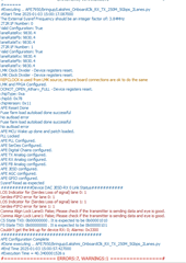
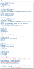
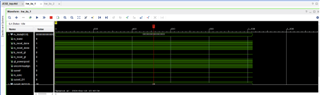
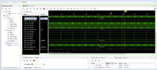
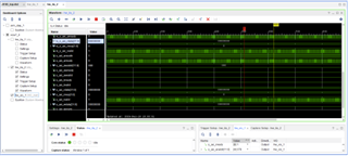
after running the script we are getting below errors.

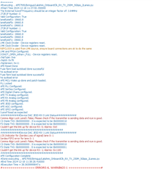
In FPGA side we can able to see tx_reset_done  and rx_reset_done signals but tx_sync and rx_sync signals are not at all coming.

CTRL_8B10B_CFG ( 03C ) =0x03010f07

CTRL_TX_ILA_CFG1 (074) =0x000f0f07

CTRL_TX_ILA_CFG1 (078) =0x00000000

 We configured these register to set the required parameter as per pg242-jesd204c-en-us-4.2 PDF


Below are the screenshots what is written into these three registers

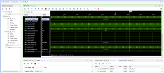
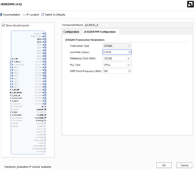
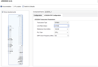
TX_core IP configuration:

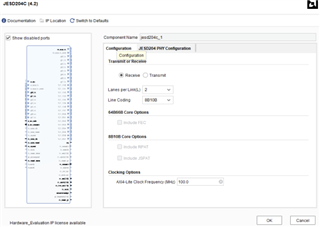
RX_core IP configuration:

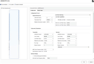
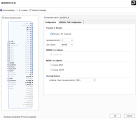
JESD phy ip configuration:

  • Hi Ajay,

    I believe there are a couple of issues here. The first is that there is a mismatch between the JESD settings on the AFE and FPGA. The lane rates are being set differently. On the AFE side the lane rate is ~19.6Gbps, which we do not recommend using with 8b10b encoding, and on the FPGA side it is 4.952Gbps. For this I would recommend changing the number of lanes or the encoding then setting the lane rate the same on the FPGA. 

    The other issue is that I think that the FPGA might be sending data on different serdes lanes that the AFE is not using. 

    Can you take a look at these issues and see if fixning them solves the problem? 

    Regards,

    David Chaparro 

  • Hi David,

    I have configured both the AFE and FPGA with a lane rate of 9.8304 Gbps. On the FPGA side, the LMFSH is set to 24810, and on the AFE side, the LMFSH is also configured to 24810 with one instance. I followed the Latte configuration script as mentioned, but I am encountering errors in the Latte log. Additionally, the FPGA side sync signal from the DAC side is not coming through, and our Rx core is not generating any sync signal either.

    Furthermore, I noticed that the SYSREF signal we are receiving from the AFE has a frequency of 3.84 MHz with a 50% duty cycle. However, from my research, the SYSREF signal should resemble a pulsed signal, not one with a 50% duty cycle. Could you kindly confirm whether the SYSREF signal we are receiving is correct?

    Can you please help me with above issue?

    #In HSDC Pro DAC tab, Select AFE79xx_2x2TX_44210; Data Rate = 245.76M
    #In HSDC Pro ADC tab, Select AFE79xx_2x2RX_44210; Data Rate = 245.76M ---> To capture 4 RX channels
    
    sysParams=AFE.systemParams
    sysParams.__init__();sysParams.chipVersion=chipVersion
    
    setupParams.skipFpga = 1 # setup FPGA (TSW14J56) using HSDC Pro 
    ##############		Top Level			##############
    sysParams.FRef			= 491.52
    sysParams.FadcRx		= 2949.12
    sysParams.FadcFb		= 2949.12
    sysParams.Fdac			= 2949.12*4
    sysParams.externalClockRx=False
    sysParams.externalClockTx=False
    													
    ##############		Digital Chain		##############
    
    		#####	RX	#####
    sysParams.ddcFactorRx	=	[12,12,12,12]			#DDC decimation factor for RX A, B, C and D
    sysParams.rxEnable		=   [True,True,False,False]
    sysParams.rxNco0		= 	[[9500,9500],			#Band0, Band1 for RXA 
    							[9500,9500],        	#Band0, Band1 for RXB 
    							[9500,9500],        	#Band0, Band1 for RXC 
    							[9500,9500]]        	#Band0, Band1 for RXD  
    
    		#####	FB	#####
    sysParams.fbEnable		=	[False,False]
    sysParams.ddcFactorFb	=	[12,12]					#DDC decimation factor for FB 1 and 2
    sysParams.fbNco0		= 	[9500,9500]				#Band0 for FB1 and FB2 
    
    		#####	TX	#####
    sysParams.ducFactorTx	=	[48,48,48,48]			#DUC interpolation factor for TX A, B, C and D
    sysParams.txEnable		=   [True,True,False,False]
    sysParams.txNco0		= 	[[9500,9500],			#Band0, Band1 for TXA 
    							[9500,9500],        	#Band0, Band1 for TXB 
    							[9500,9500],        	#Band0, Band1 for TXC 
    							[9500,9500]]        	#Band0, Band1 for TXD
    
    
    ##############		JESD		##############
    
    		#####	ADC-JESD	#####
    sysParams.jesdSystemMode= [3,3]
    													#SystemMode 0:	2R1F-FDD						; rx1-rx2-fb -fb
    													#SystemMode 1:	1R1F-FDD						; rx -rx -fb -fb
    													#SystemMode 2:	2R-FDD							; rx1-rx1-rx2-rx2
    													#SystemMode 3:	1R								; rx -rx -rx -rx
    													#SystemMode 4:	1F								; fb -fb- fb -fb
    													#SystemMode 5:	1R1F-TDD						; rx/fb-rx/fb-rx/fb-rx/fb
    													
    sysParams.jesdTxProtocol= [0,0]						# 0 - 8b/10b encoding; 2 - 64b/66b encoding 
    sysParams.LMFSHdRx		= ["24410","24410","24410","24410"]   #changed by Lakshmi ["44210","44210","44210","44210"] 
    													# The 2nd and 4th are valid only for jesdSystemMode values in (0,2).
    													# For other modes, select 4 converter modes for 1st and 3rd.
    sysParams.LMFSHdFb		= ["14810","14810"]
    
    sysParams.rxJesdTxScr	= [True,True,True,True] #changed by Lakshmi
    sysParams.fbJesdTxScr	= [True,True]
    
    sysParams.rxJesdTxK		= [16,16,16,16]
    sysParams.fbJesdTxK		= [16,16]
    
    sysParams.jesdTxLaneMux	= [0,1,2,3,4,5,6,7]			# Enter which lanes you want in each location. 
    													# For example, if you want to exchange the first two lines of each 2T,
    													#		this should be [[1,0,2,3],[5,4,6,7]]
    
    		#####	DAC-JESD	#####
    sysParams.jesdRxProtocol= [0,0]
    sysParams.LMFSHdTx		= ["24410","24410","24410","24410"]  
    sysParams.jesdRxLaneMux	= [0,1,2,3,4,5,6,7]			# Enter which lanes you want in each location.
    sysParams.serdesRxLanePolarity = [1,1,0,0,1,1,0,0]													# For example, if you want to exchange the first two lines of each 2R
    													#		this should be [[1,0,2,3],[5,4,6,7]]
    sysParams.jesdRxRbd		= [4, 4]
    sysParams.jesdRxScr		= [True,True,True,True]
    sysParams.jesdRxK		= [16,16,16,16]
    
    		#####	JESD Common	#####
    	
    sysParams.jesdABLvdsSync= True
    sysParams.jesdCDLvdsSync= True
    sysParams.syncLoopBack	= True	#JESD Sync signal is connected to FPGA
    
    ##############		GPIO		##############
    sysParams.gpioMapping	= {
    						'H8': 'ADC_SYNC0',
    						'H7': 'DAC_SYNC0',  	#'ADC_SYNC1',
    						'N8': 'ADC_SYNC2',
    						'N7': 'ADC_SYNC3',
    						'H9': 'ADC_SYNC1',		#'DAC_SYNC0',
    						'G9': 'DAC_SYNC1',
    						'N9': 'DAC_SYNC2',
    						'P9': 'DAC_SYNC3',
    						'P14': 'GLOBAL_PDN',
    						'K14': 'FBABTDD',
    						'R6': 'FBCDTDD',
    						'H15': ['TXATDD','TXBTDD'],
    						'V5': ['TXCTDD','TXDTDD'],
    						'E7': ['RXATDD','RXBTDD'],
    						'R15': ['RXCTDD','RXDTDD']}
    
    ##############		LMK Params		##############
    lmkParams.pllEn			= True
    lmkParams.inputClk		= 983.04 # Valid only when lmkParams.pllEn = False
    lmkParams.lmkFrefClk	= True
    setupParams.fpgaRefClk	= 245.76 # Should be equal to LaneRate/40 for TSW14J56
    
    ##############		Logging		##############
    logDumpInst.setFileName(ASTERIX_DIR+DEVICES_DIR+r"\Afe79xxPg1.txt")
    logDumpInst.logFormat=0x0 #Modify to 0x1 to save register scequence to log file. Script takes more time to execute.
    logDumpInst.rewriteFile=1
    logDumpInst.rewriteFileFormat4=1
    device.optimizeWrites=0
    device.rawWriteLogEn=1
    
    device.delay_time = 0
    
    AFE.deviceBringup()
    
    AFE.TOP.overrideTdd(15,3,15)	# bit-wise; 4R,2F,4T

    log results:

     ...

  • Hi Ajay,

    There are two issues that I see. The first is that if you would like to use a CMOS sync signal then the following two parameters should be set to 'False'.

    sysParams.jesdABLvdsSync= True
    sysParams.jesdCDLvdsSync= True

    The second issue is that the LOS error that you are seeing indicates that the FPGA may be sending data on different serdes lanes. Can you confirm that your FPGA is configured to send data on the FPGA lanes connected to SRX1 and SRX2?

    Regards,

    David Chaparro 

  • Hi David,

    Regarding the SerDes lane connection, we are currently transmitting the data to SRX1 and SRX2 only.

    As per your instructions, we have updated the two parameters to "false." However, the sync signal is still not being received, and we are encountering errors in the Latte log. Additionally, I had previously inquired about the SYSREF signal in my last query. Could you kindly confirm its status?

  • Hi David,

    We have the DC135-AFE7950EVM board; however, we were unable to locate its schematic. As a result, we used the DC150A-AFE7950EVM schematic as a reference. Could you kindly confirm if this approach is acceptable? If not, could you please direct me to where I can find the required schematic? Is it possible to share the link for the schematic DC135A board.