This thread has been locked.

If you have a related question, please click the "Ask a related question" button in the top right corner. The newly created question will be automatically linked to this question.

AFE7769D: SPI communication Problem

Part Number: AFE7769D

Tool/software:

Hello,


We have a problem with communicating with AFE7769D.
We use the Agilex5(Intel) CPU as a master.
I have some questions like below.

  1. Power, Clock
    According to datasheet, AFE7769D is entered Power On Reset Mode after H/W reset.
    To communicate(SPI) with AFE7769D properly, I think that AFE7769D should be reset and initialized properly first.
    For the porper initialization, the power condition and reference clock(to AFE7769D) should be satisfied.
    By the way, this may seem obvious, but can you explain why the reference clock input to AFE7769D is important?
    Because my hardware engineer said that the reference clock doesn't mattter.

    The power has been verified to meet the conditions described in Section 7.3 Recommended Operating Conditions.
    Should the power conditions described in Section 7.1 Absolute Maximum Ratings also be met?

  2. SPI mode
    If you look at the library provided with the SDK, the code inside the SPI Write/Read functions are empty.
    (It is described to "/* TBD: User domain */" as a annotation.)
    It seems that this is a part that needs to be written by library user(to match their device).
    //CAFE/Afe77xxDUser/Src/tiAfe77D_baseFunc.c
    //...
    TI_AFE_API_COMP uint8_t AFE77DFNP(afeSpiRawWrite)(AFE77D_INST_TYPE afeInst, uint16_t addr, uint8_t data)
    {
        afeLogDbg("WRITE: Address: 0x%X, data: 0x%X", addr, data);
        /* TBD: User domain */
        uint8_t status = ftdi_writeReg(addr, data);
        // AFE77D_FUNC_EXEC(AFE77DFNP(afeWaitMs)(afeInst, 20);
        if (status == 0)
            return TI_AFE_RET_EXEC_PASS;
        else
            return TI_AFE_RET_EXEC_FAIL;
    }
    
    /**
        @brief AFE SPI read driver function.
        @details AFE SPI read driver function and returns the read value as pointer. The contents of this function should be replaced by host SPI driver function.
        @param afeInst AFE Instance of AFE77D_INST_TYPE type
        @param addr Address to be read from.
        @param readVal Pointer return of the value read.
        @return Returns if the function execution passed or failed.
    */
    TI_AFE_API_COMP uint8_t AFE77DFNP(afeSpiRawRead)(AFE77D_INST_TYPE afeInst, uint16_t addr, uint8_t *readVal)
    {
        /* TBD: User domain */
        *readVal = 0;
        // AFE77D_FUNC_EXEC(AFE77DFNP(afeWaitMs)(afeInst, 20);
        *readVal = ftdi_readReg(0x8000 | addr);
        afeLogDbg("READ: Address: 0X%X, Read Val: 0X%X", addr, *readVal);
        return TI_AFE_RET_EXEC_PASS;
    }
    //...

    In order to set up SPI communication, it seems that you need to change the SPI mode to match the slave, as in the URLs below.
    https://e2e.ti.com/support/amplifiers-group/amplifiers/f/amplifiers-forum/1338667/afe031-spi-communication-problem/5126881?tisearch=e2e-sitesearch&keymatch=AFE7%20spi%20lsb#5126881
    https://e2e.ti.com/support/data-converters-group/data-converters/f/data-converters-forum/1281553/afe881h1evm-spi-read-issue-with-afe-board?tisearch=e2e-sitesearch&keymatch=afe%2520spi%2520read#

    In the data sheet, it seems that I need to use 1 for writing to slave device and 0 for read from slave device.
    In the 8.3.17. Serial Peripheral Interface (SPI) section, it is described as follows.
    Data is input into the device with the rising edge of SCCLK.
    Data is output from the device on the falling edge of SCLK.
    The SPI registers-except for global register GLOBAL0 and GLOBAL1 - are reset by writing a "1" to GLOBAL_SOFT_RESET in the GLOBAL0 register.

    What I'm wondering is, is it correct to set SPI mode to 1 when writing from Master and to set SPI mode to 0 when reading from Master?
    I am using below spi configurations:
     - SCLK: 10MHz
     - CS : Active Low
     - SPI Mode: 1(write), 0(read)
     - Data Order: LSB first
     - Master device: Agilex5(Intel)

Regards,

Jung.

  • Hi Jung,

    By the way, this may seem obvious, but can you explain why the reference clock input to AFE7769D is important?
    Because my hardware engineer said that the reference clock doesn't mattter.

    Just for initial SPI communication, to read device ID or device version, reference clock does not matter.

    The reference clock and sysref starts to play role when AFE is being configured for the desired operation in platform.

    The power has been verified to meet the conditions described in Section 7.3 Recommended Operating Conditions.
    Should the power conditions described in Section 7.1 Absolute Maximum Ratings also be met?

    Absolute Maximum Rating just convey the worst case supply voltages that device can handle incase any power rails glitches occur in the system. Beyond these voltages, AFE may get permanently damaged.

    So using nominal voltages from section 7.3 is sufficient.

    If you look at the library provided with the SDK, the code inside the SPI Write/Read functions are empty.
    (It is described to "/* TBD: User domain */" as a annotation.)
    It seems that this is a part that needs to be written by library user(to match their device).

    Yes, this is correct. We use FTDI chip on AFE EVB, for which we have added the FTDI related code, you must replace that line to match whatever processor can provide.

    For SPI setting:

    1. SCLK Frequency: 10MHz
    2. CS: Active LOW
    3. SPI Mode: 0 to Write to AFE, 1 to Read from AFE
    4. Data Order: MSB First
    5. Data Latch: Positive Edge to Write to AFE, Negative Edge to Read from AFE.
    6. Master Device: FTDI or Agilex as long as the conditions are met correctly.
  • Hello, Neeraj Kumar Sharma.

    Thank you for the answer.

    I modified SPI configurations as you mentioned.(MSB first, SPI Mode)

    I tried to read Chip ID. But response data seems that invalid.

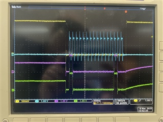
    When I try to read operation, the oscilloscope waveform looks like this:

    CH1(yellow): CS

    CH2(blue): SCLK

    CH3(purple): MOSI

    CH4(green): MISO

    In this waveform, the third bit from the end is set to 1, so 0x8004 is transmitted.

    (Because this data is read command, I set MSB to 1.)

    But response data seems that invalid.

    Could you advice me about what I should do something more?

    Regards,

    Jung.

  • Hi Jung,

    To add more to the SPI settings, the Address length is 16 bits and data length is 8 bits. So the packet length must be total of 24 bits. Please record the waveforms for 24 clock cycles.

  • Hello, Neeraj Kumar Sharma

    Thank you for the answer.

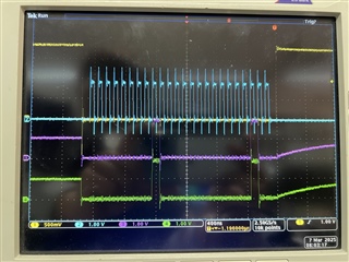
    I trided to transfer 24bit width data.

    To align data to 24bit width, I sent 0x008004.

    However, it seems that the response data is still invalid.

    The waveform is like below.

    I would appreciate it if you could let me know what other settings I should check.

    Regards,

    Jung.

  • Hi Jung,

    To align data to 24bit width, I sent 0x008004.

    Please refer to Figure 8-128: SPI READ BUS CYCLE from datasheet.

    You must actually send 0x8004 in first 16 clock cycle and then keep the clock active for 8 more cycles, to receive the data. This effectively makes the packet length as 24 bits.