LMX8410L: LMX8410L Temperature issue

Part Number: LMX8410L

Tool/software:

Hi, I'll give you some context first:
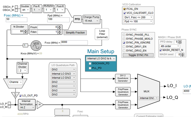
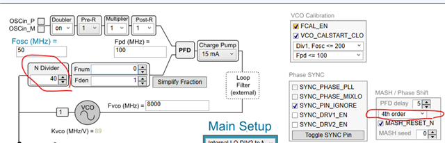
We are using this demodulator in a custom board because we want a LO of 7.2 GHz. We are using internal configuration with the VCO divided by CH_DIV.

The OSCIN is 50MHz and it comes through LVDS at 3.5mA with a DC Level of 1.6V per line. Then we use the doubler to take it to 100MHz.

For the Power Up Sequence we are manipulating the registers as It shows below: (I put only the registers that allow special configuration, the rest or them were obtained via TICS Pro and confirmed with the Datasheet as it recommends).

REGISTER DATA (hex)
0 0x665C
1 0x080B
9 0x1604
10 0x1088
11 0x0018
14 0x13F0
36 0x0090
37 0x8204
38 0x0000
39 0x0001
40 0x0000
41 0x0000
42 0x0000
43 0x0000
44 0x1FA0
46 0x07FC
75 0x0200
79 0x0000
80 0x0009
81 0x09D7
83 0x3221
84 0x1903
94 0x8080
95 0x0000
103 0x2C00
126 0x0000

We have checked the registers a lot of times, just to make sure we've are coding everything well, and it still getting hot (around 120°C). The Enable line comes from a PIC that we are programming with MPLAB and it communicates with the PLL via SPI, and the pin configuration is like in the Evaluation Board. 


Do you know what else can we check? Any recommendation? Is it common to having temperature issues with this model? Please, if you read the code and found something, if you had experience with this chip, it would be really useful.

  • This was my configuration in TICS Pro to Extract the registers and programmed the PIC via SPI, didn't work. Lock detected does not appear.

  • Update: I solved some issues with registers. For some reason TICS Pro showed some registers first, and I re-changed the parameters and showed different registers, I applied those new ones, and now the PLL is able to Lock. The problem now is that when the PLL gets Locked, the temperature starts increasing. So now my problem is not about the registers, but the temperature. This temperature is on the chip, not on the board. 
    If you know something about it, I will be more than glad to receive your advices. 

  • Hi Carlos,

    This device consumes 3.3V x 650mA + 5V x 130mA = 2.795W of power. It is not surprising that the device is very hot. How many layer you have on your pcb? Do you have enough copper plane to dissipate the heat generated from the device? If you can measure the board temperature, we can estimate the die temperature. As long the die temperature is less than the junction temperature, it is fine.

  • Hi Noel,
    Thank you so much for answering. We have 8 layers in our board. 

    1. Top - Signal
    2. Ground
    3. Signal
    4. Ground
    5. Power
    6. Power
    7. Ground
    8. Bottom - Signal

    The problem is that, when the PLL gets Locked, the temperature starts increasing, and when it reaches around 40°C, the PLL loses the Lock, but the temperature is still increasing till 120°C that is the max we have ever read.

  • Hi Carlos,

    What temperature? is it board temperature, device surface temperature or what? Is the current consumption normal?

  • Hi Noel,
    As I told you, this is the chip temperature. By now, we have solved many problems with the temperature. The answer you provided about the current consumption and 2.79W led us to check the datasheet and with an adjustment in our hardware, the device is not reaching those high temperatures anymore. Is around 70°C, 80°C so now we assume is normal. The problem we are facing now, is as follows:

    We programmed a whole set up for the device, writing to the correct registers to Initialize, Enable and change frequency on the device. Currently, we don't know what to do cause we are initializing the device, enabling it, and it gets locked. But when we re-do this process, the PLL keeps the lock even when it has not been re-enabled yet, so it basically stays in an infinite lock till we turn off the voltage. 

    Since I commented that I solved the problem with the registers, I would like to add a new table with the new registers I obtained from TICs PRO, just to check if there is something else wrong. those who are not in this table, were settled to zero.

    Register Address Value
    R127 (INIT1) 0x7F  0003
    R115 0x73  0800
    R103 0x67  2C00
    R96 0x60  9000
    R94 0x5E  8080
    R88 0x58  0003
    R84 0x54  1900
    R83 0x53  6A00
    R82 0x52  0023
    R81 0x51  0310
    R80 0x50  0009
    R78 0x4E  0200
    R58 0x3A  8000
    R44 0x2C  00A4
    R39 0x27  0001
    R37 0x25  0500
    R36 0x24  0050
    R14 0x0E  0070
    R11 0x0B  0010
    R10 0x0A  0080
    R9 0x09  1000
    R0 0x00  000C
  • Hi Carlos,

    Since you use TICS Pro, please send me the .tcs configuration file, thanks.

  • ForTexasForum.tcs

    Hi Noel, 
    Here is the .tcs file. Thank you very much.

  • (Update)
    What we currently doing is: 

    Supplying the device with 3.3V, activating the Enable process, starting the initialization in descending order (as the table I showed few messages back), then, the Calibration (with the 3rd bit of register R1), and when the device gets locked, we activate the Enables from the DCOC. Additionally, we are seeing the VCO Calibration bit, but despite that, when we deactivate the Enable, we're still seeing the MUX OUT on. We can only stop the lock by turning off the supply voltage completely. 

    I hope this will make it clearer. Thanks.

  • Hi Carlos,

    Unfortunately, I still don't understand your problem. 

    Is the PLL unable to lock? Are you not able to change the frequency? Or something else?

    Your configuration has an issue. There is restriction on the PLL_N value which is dependent on the MASH order.

    The restriction is like this.

    So for PLL_N=40, change the MASH order to 3rd order and change the PFD delay accordingly to 3.

  • Hi Noel,

    We are working with a custom board that uses the LMX8410 as a demodulator, controlled via SPI by a PIC microcontroller. The configuration we attach from TICs Pro is the initialization we currently apply to the demodulator. After this initialization, we don’t change any other settings.

    Our initialization sequence is as follows:

    1. Enable the demodulator.
    2. Write to registers 127 and 6 as recommended in the datasheet.
    3. Trigger a reset through Register 0.
    4. Write all registers in descending order.
    5. Wait 10 ms, check the VCO lock status, and then enable DCOC calibration.

    The temperature issue we had before is already solved, but now we are facing two main problems:

    We check the VCO lock status through the MUXout pin. It indicates that there is lock after initialization, but if we disable the enable pin (set it to 0 V), the MUXout pin still shows a lock condition.

    We are not observing the expected IF output corresponding to LO – RF. We suspect this could be related to incorrect configuration of mash order and delay (DLY) with respect to our VCO and PFD settings.

    Our setup: PFD = 100 MHz, 50 MHz at OSCin with the doubler enabled.

    • We target 6.5 GHz at the LO, so we aim for 13,000 MHz at the VCO with CHDIV2 enabled.
    • Could you please help us with the following points?
    • Why does the MUXout pin (VCO cal) remain HIGH even after the enable pin is de-asserted?
    • Can you confirm whether our configuration is correct for achieving the LO output through CHDIV2, and if the rest of the setup looks valid?

    The table information about N and MASH Order restrictions is clear, however, the file I sent you was using a 8000 Fvco Frequency, with N = 40, and MASH = 4th, DLY = 5. According to this table, this values should be correct. What would be the configuration for the values we are aiming? With N between 80 and 150.

    I hope this clarifies our issue. If anything is not clear, I will be glad to provide further details.

    Thanks a lot,
    Best regards,

  • Hi Carlos,

    After initialization and PLL lock, when you set CE pin = 0, did you see a significant current drop?

    The min. N is 44 with 4th order MASH.

    Let me check if I have a board in the lab I can try. 

  • Hi Noel,
    We know that the voltage drops a little bit and the PLL heats between 70°C and 80°C, but we already assume that this temperature is normal. 

  • Hi Carlos,

    I don't have the board in the lab, I rely on you to debug.

    If the CE pin (pin 1) controls the whole chip, then making it =0 should reduce the current consumption significantly. Did you see this big change in current? If the CE pin controls only to the demodulator but not the synthesizer, you should still see maybe 300mA of current which is consumed by the synthesizer. If you program PLL_PD = 1 now, then MUXOUT should become 0V as the synthesizer is powered down. 

  • Hi Noel,

    We implemented a method enabling and disabling the Power Down, establishing the R0 fourth bit = 1 for Activated, and = 0 for Deactivated. We tested this method and the Lock state is still On. The current is still in the same value, but we saw that turning off the Enable, generates a current drop, approximately of 500mA  but the Lock state is always there and the only way to remove it is turning off the voltage that feeds the entire PLL.

  • Hi Carlos,

    PLL_PD is located in R0, bit 0. 

  • Hi Noel,
    We so sorry, there was a confusion writing our previous answer. Effectively, we are writing to R0 bit 0. Our configuration is 0x0004 and when we activate it is 0x0005, and however, as we told you before, the problem with the Lock Status is still there. 

    Could you please check if the configuration we are using with the rest of registers is ok or do you find something else wrong? Our tests include introducing a signal into the RF IN pin, and measuring the output pins (QP, QM, PQ, PM). Our LO configuration says we are at 6.5GHz, but the tests say we are around 8GHz and we cannot find why. Here's a table with some results we've obtained if it's useful:

    RF IN IF OUT
    6.9 GHz 1.088 GHz
    6.8 GHz 1.189 GHz 
    6.7GHz 1.289 GHz 
    7 GHz 970 MHz