This thread has been locked.

If you have a related question, please click the "Ask a related question" button in the top right corner. The newly created question will be automatically linked to this question.

AFE7950EVM: LATTE 2.9 issue & rollback 2.8 issue

Part Number: AFE7950EVM
Other Parts Discussed in Thread: TSW14J58EVM

Hi team,

my customer used LATTE 2.8 for some time without any issues. They upgraded to version 2.9 recently and experienced the following issue:

RX/TX Channel Frequency Map on the config page is not selectably anymore (permanently greyed out).

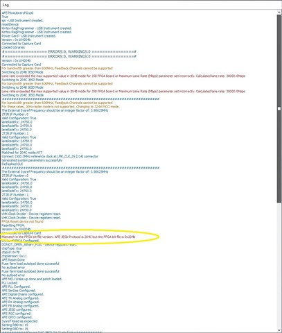
They wanted to roll back to version 2.8, but after installing, the following error message came up:
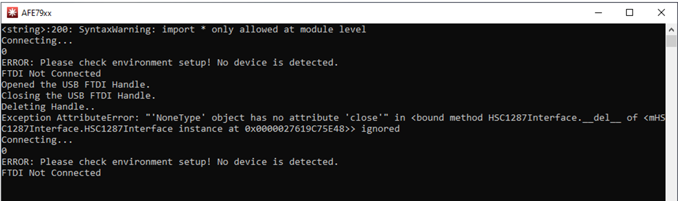
image.png

The GUI then does not establish connection to the TSW14J58EVM:

image.png

They tried multiple reboots and uninstalling/installing the software, but without success?

Can you help?

Best regards

  • Hi Franziskus,

    I would recommend that they stay with version 2.9. I will check with the team on why that button is greyed out. 

    While we are debugging this the customer can use the parameter below to change between the Rx and Tx frequency map. This can be set in the command line window of Latte. 

    configGeniGuiClass.channel = 0 # This sets it to Rx

    configGeniGuiClass.channel = 1# This set is to Tx

    Regards,

    David Chaparro 

  • Thanks David!

    Here's new information:

    -----------------------------

    I was able to work around the problem with the FTDI driver that I returned to an earlier state (before installing the latte SW) using Windows recovery point. Can install and start both V2.8 and V2.9 as an alternative. But now I have the following problem: My test configuration (see screenshot) which I have on 22.10. Having successfully got to run has now neither worked with the V2.8 nor with the V2.9. My test configuration: With LMK input=1500MHz

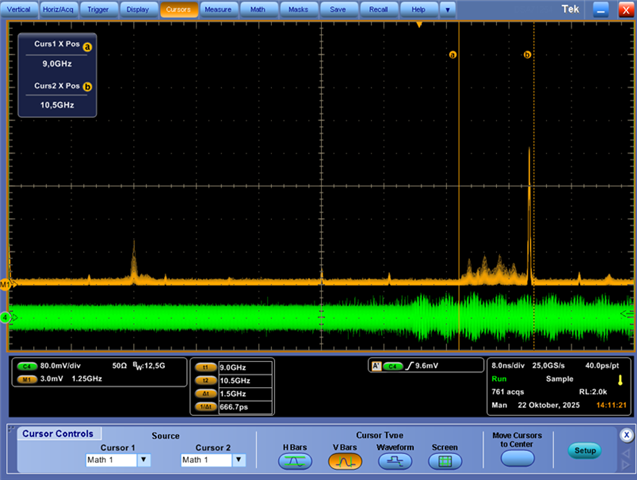
    I have captured the TX signal:

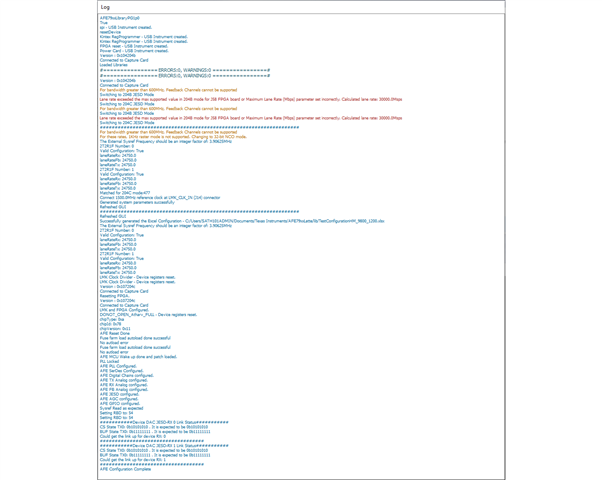
    Here's the log file of successful initialization:

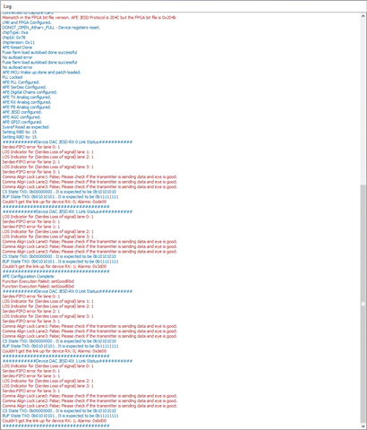
    Now, verion 2.8 gives the following error during initialization:

    And version 2.9 crashes during initialization:

    I found a significant difference in initialization in the log file (compared to the successful run at that time). There probably is an issue with the FPGA bitfile (of the TSW14J58EVM??) – How can I fix this (I already installed the latte software fresh) ?

    Here's the full log file for the error case:

    AFE79xxLibraryPG1p0
    True
    spi - USB Instrument created.
    resetDevice
    Kintex RegProgrammer - USB Instrument created.
    Kintex RegProgrammer - USB Instrument created.
    Power Card - USB Instrument created.
    Version : 0x104204b
    Connected to Capture Card
    Loaded Libraries
    #================ ERRORS:0, WARNINGS:0 ================#
    #================ ERRORS:0, WARNINGS:0 ================#
    Version : 0x104204b
    Connected to Capture Card
    For bandwidth greater than 600MHz, Feedback Channels cannot be supported
    Switching to 204B JESD Mode
    Lane rate exceeded the max supported value in 204B mode for J58 FPGA board or Maximum Lane Rate (Mbps) parameter set incorrectly. Calculated lane rate: 30000.0Msps
    Switching to 204C JESD Mode
    For bandwidth greater than 600MHz, Feedback Channels cannot be supported
    Switching to 204B JESD Mode
    Lane rate exceeded the max supported value in 204B mode for J58 FPGA board or Maximum Lane Rate (Mbps) parameter set incorrectly. Calculated lane rate: 30000.0Msps
    Switching to 204C JESD Mode
    ###################################################################
    For bandwidth greater than 600MHz, Feedback Channels cannot be supported
    For these rates, 1KHz raster mode is not supported. Changing to 32-bit NCO mode.
    The External Sysref Frequency should be an integer factor of: 3.90625MHz
    2T2R1F Number: 0
    Valid Configuration: True
    laneRateRx: 24750.0
    laneRateFb: 24750.0
    laneRateTx: 24750.0
    2T2R1F Number: 1
    Valid Configuration: True
    laneRateRx: 24750.0
    laneRateFb: 24750.0
    laneRateTx: 24750.0
    Matched for 204C mode:477
    Connect 1500.0MHz reference clock at LMK_CLK_IN (J14) connector
    Generated system parameters successfully
    Refreshed GUI
    ###################################################################
    The External Sysref Frequency should be an integer factor of: 3.90625MHz
    2T2R1F Number: 0
    Valid Configuration: True
    laneRateRx: 24750.0
    laneRateFb: 24750.0
    laneRateTx: 24750.0
    2T2R1F Number: 1
    Valid Configuration: True
    laneRateRx: 24750.0
    laneRateFb: 24750.0
    laneRateTx: 24750.0
    LMK Clock Divider - Device registers reset.
    LMK Clock Divider - Device registers reset.
    FPGA Reset device not found
    Resetting FPGA.
    Version : 0x104204b
    Connected to Capture Card
    Mismatch in the FPGA bit file version. AFE JESD Protocol is 204C but the FPGA bit file is 0x204b
    LMK and FPGA Configured.
    DONOT_OPEN_Atharv_FULL - Device registers reset.
    chipType: 0xa
    chipId: 0x78
    chipVersion: 0x11
    AFE Reset Done
    Fuse farm load autoload done successful
    No autload error
    Fuse farm load autoload done successful
    No autload error
    AFE MCU Wake up done and patch loaded.
    PLL Locked
    AFE PLL Configured.
    AFE SerDes Configured.
    AFE Digital Chains configured.
    AFE TX Analog configured.
    AFE RX Analog configured.
    AFE FB Analog configured.
    AFE JESD configured.
    AFE AGC configured.
    AFE GPIO configured.
    Sysref Read as expected
    Setting RBD to: 15
    Setting RBD to: 15
    ###########Device DAC JESD-RX 0 Link Status###########
    Serdes-FIFO error for lane 0: 1
    LOS Indicator for (Serdes Loss of signal) lane 1: 1
    Serdes-FIFO error for lane 1: 1
    LOS Indicator for (Serdes Loss of signal) lane 2: 1
    Serdes-FIFO error for lane 2: 1
    LOS Indicator for (Serdes Loss of signal) lane 3: 1
    Serdes-FIFO error for lane 3: 1
    Comma Align Lock Lane2: False; Please check if the transmitter is sending data and eye is good.
    CS State TX0: 0b00000000 . It is expected to be 0b10101010
    BUF State TX0: 0b01010101 . It is expected to be 0b11111111
    Couldn't get the link up for device RX: 0; Alarms: 0xfe00
    ###################################
    ###########Device DAC JESD-RX 1 Link Status###########
    LOS Indicator for (Serdes Loss of signal) lane 0: 1
    Serdes-FIFO error for lane 0: 1
    Serdes-FIFO error for lane 1: 1
    LOS Indicator for (Serdes Loss of signal) lane 2: 1
    Serdes-FIFO error for lane 2: 1
    LOS Indicator for (Serdes Loss of signal) lane 3: 1
    Comma Align Lock Lane2: False; Please check if the transmitter is sending data and eye is good.
    Comma Align Lock Lane3: False; Please check if the transmitter is sending data and eye is good.
    CS State TX0: 0b00000000 . It is expected to be 0b10101010
    BUF State TX0: 0b01010101 . It is expected to be 0b11111111
    Couldn't get the link up for device RX: 1; Alarms: 0x7d00
    ###################################
    AFE Configuration Complete
    Function Execution Failed: setGoodRbd
    Function Execution Failed: setGoodRbd
    ###########Device DAC JESD-RX 0 Link Status###########
    Serdes-FIFO error for lane 0: 1
    LOS Indicator for (Serdes Loss of signal) lane 1: 1
    Serdes-FIFO error for lane 1: 1
    LOS Indicator for (Serdes Loss of signal) lane 2: 1
    Serdes-FIFO error for lane 2: 1
    LOS Indicator for (Serdes Loss of signal) lane 3: 1
    Serdes-FIFO error for lane 3: 1
    Comma Align Lock Lane2: False; Please check if the transmitter is sending data and eye is good.
    CS State TX0: 0b00000000 . It is expected to be 0b10101010
    BUF State TX0: 0b01010101 . It is expected to be 0b11111111
    Couldn't get the link up for device RX: 0; Alarms: 0xfe00
    ###################################
    ###########Device DAC JESD-RX 1 Link Status###########
    LOS Indicator for (Serdes Loss of signal) lane 0: 1
    Serdes-FIFO error for lane 0: 1
    Serdes-FIFO error for lane 1: 1
    LOS Indicator for (Serdes Loss of signal) lane 2: 1
    Serdes-FIFO error for lane 2: 1
    LOS Indicator for (Serdes Loss of signal) lane 3: 1
    Serdes-FIFO error for lane 3: 1
    Comma Align Lock Lane2: False; Please check if the transmitter is sending data and eye is good.
    Comma Align Lock Lane3: False; Please check if the transmitter is sending data and eye is good.
    CS State TX0: 0b00000000 . It is expected to be 0b10101010
    BUF State TX0: 0b01010101 . It is expected to be 0b11111111
    Couldn't get the link up for device RX: 1; Alarms: 0xfd00
    ###################################

    -----------------------------

    Best regards

  • Another update:

    ----------------------------------------

    I have now reinstalled the Latte SW V2.9 on another computer and experimented with the settings. With this I could further circle the problem but now no more!

    With a narrow band configuration that works with JESD204B setting, everything runs normal.
    For larger bandwidths that require JESD204C (Autoselect JESD coding), the initialization then aborts with errors even though the configuration has been successfully validated (Validate Settings OK).
    The following line in the log file is probably decisive here:

    Mismatch in the FPGA bit file version. AFE JESD Protocol is 204C but the FPGA bit file is 0x204b

    In my tests at the time with the 2.8 bar, the automatic switch to JESD204C worked without any problems.
    I wonder if V2.9 is a bug here or the EVM (probably the TSW14J58EVM ?) Has a HW defect.

    Would you have the option of testing the following configuration with V2.9?

    Default settings after starting the latte software (Part No. AFE7950-4T4R2F, RX/TX center frequency = 9600MHz, FADC = 2949.12MHz), With the following amendment:

    • -Autoselect JESD Coding
    • -Bandwidth = 500MHz

    A 10MHz/10dBm clock is required at the LMK input here!
    See also the screenshot of the Latte Configuration Windows in the appendix.
    The complete log file as a text file is also attached.

    AFE79xxLibraryPG1p0
    True
    spi - USB Instrument created.
    resetDevice
    Kintex RegProgrammer - USB Instrument created.
    Kintex RegProgrammer - USB Instrument created.
    Power Card - USB Instrument created.
    Version : 0x104204b
    Connected to Capture Card
    Loaded Libraries
    #================ ERRORS:0, WARNINGS:0 ================#
    #================ ERRORS:0, WARNINGS:0 ================#
    Version : 0x104204b
    Connected to Capture Card
    ###################################################################
    Switching to 204B JESD Mode
    Lane rate exceeded the Maximum Lane Rate(Mbps) value entered.
    Switching to 204C JESD Mode
    The External Sysref Frequency should be an integer factor of: 3.84MHz
    2T2R1F Number: 0
    Valid Configuration: True
    laneRateRx: 24330.24
    laneRateFb: 24330.24
    laneRateTx: 24330.24
    2T2R1F Number: 1
    Valid Configuration: True
    laneRateRx: 24330.24
    laneRateFb: 24330.24
    laneRateTx: 24330.24
    Matched for 204C mode:489
    Connect 10MHz reference clock at LMK_CLK_IN (J14) connector, for EVM synchronization
    Generated system parameters successfully
    Refreshed GUI
    ###################################################################
    The External Sysref Frequency should be an integer factor of: 3.84MHz
    2T2R1F Number: 0
    Valid Configuration: True
    laneRateRx: 24330.24
    laneRateFb: 24330.24
    laneRateTx: 24330.24
    2T2R1F Number: 1
    Valid Configuration: True
    laneRateRx: 24330.24
    laneRateFb: 24330.24
    laneRateTx: 24330.24
    LMK Clock Divider - Device registers reset.
    LMK Clock Divider - Device registers reset.
    REFCLOCK is used from LMK source, ensure board connections are ok to do the same
    FPGA Reset device not found
    Resetting FPGA.
    Version : 0x104204b
    Connected to Capture Card
    Mismatch in the FPGA bit file version. AFE JESD Protocol is 204C but the FPGA bit file is 0x204b
    LMK and FPGA Configured.
    DONOT_OPEN_Atharv_FULL - Device registers reset.
    chipType: 0xa
    chipId: 0x78
    chipVersion: 0x11
    AFE Reset Done
    Fuse farm load autoload done successful
    No autload error
    Fuse farm load autoload done successful
    No autload error
    AFE MCU Wake up done and patch loaded.
    PLL Locked
    AFE PLL Configured.
    AFE SerDes Configured.
    AFE Digital Chains configured.
    AFE TX Analog configured.
    AFE RX Analog configured.
    AFE FB Analog configured.
    AFE JESD configured.
    AFE AGC configured.
    AFE GPIO configured.
    Sysref Read as expected
    Setting RBD to: 15
    Setting RBD to: 15
    ###########Device DAC JESD-RX 0 Link Status###########
    Serdes-FIFO error for lane 0: 1
    LOS Indicator for (Serdes Loss of signal) lane 1: 1
    Serdes-FIFO error for lane 1: 1
    Comma Align Lock Lane1: False; Please check if the transmitter is sending data and eye is good.
    CS State TX0: 0b00000000 . It is expected to be 0b00001010
    BUF State TX0: 0b00000101 . It is expected to be 0b00001111
    Couldn't get the link up for device RX: 0; Alarms: 0x3200
    ###################################
    ###########Device DAC JESD-RX 1 Link Status###########
    LOS Indicator for (Serdes Loss of signal) lane 0: 1
    Serdes-FIFO error for lane 0: 1
    Serdes-FIFO error for lane 1: 1
    Comma Align Lock Lane0: False; Please check if the transmitter is sending data and eye is good.
    CS State TX0: 0b00000000 . It is expected to be 0b00001010
    BUF State TX0: 0b00000101 . It is expected to be 0b00001111
    Couldn't get the link up for device RX: 1; Alarms: 0x3100
    ###################################
    AFE Configuration Complete
    Function Execution Failed: setGoodRbd
    Function Execution Failed: setGoodRbd
    Function Execution Failed: setGoodRbd
    ###########Device DAC JESD-RX 0 Link Status###########
    Serdes-FIFO error for lane 0: 1
    LOS Indicator for (Serdes Loss of signal) lane 1: 1
    Serdes-FIFO error for lane 1: 1
    Comma Align Lock Lane1: False; Please check if the transmitter is sending data and eye is good.
    CS State TX0: 0b00000000 . It is expected to be 0b00001010
    BUF State TX0: 0b00000101 . It is expected to be 0b00001111
    Couldn't get the link up for device RX: 0; Alarms: 0x3200
    ###################################
    ###########Device DAC JESD-RX 1 Link Status###########
    LOS Indicator for (Serdes Loss of signal) lane 0: 1
    Serdes-FIFO error for lane 0: 1
    Serdes-FIFO error for lane 1: 1
    Comma Align Lock Lane0: False; Please check if the transmitter is sending data and eye is good.
    CS State TX0: 0b00000000 . It is expected to be 0b00001010
    BUF State TX0: 0b00000101 . It is expected to be 0b00001111
    Couldn't get the link up for device RX: 1; Alarms: 0x3100
    ###################################

    ----------------------------------------

    Best regards

  • Hi Franziskus, 

    I will test this on my side to verify that it should auto-select the appropriate FW versioin. 

    In the mean time the customer can manually select the 204c FW by changing a jumper setting. For the 204c FW they can put jumper J35, on the TSW14J58EVM, in the 1-2 position. 

    Regards,

    David Chaparro 

  • David,

    when they put the jumper on position 1-2, the error message concerning the bit-file is gone. Unfortunately, initialization at 1000 MHz bandwidth still triggers a fault  of the JESD-Interface, see file below.

    AFE79xxLibraryPG1p0
    True
    spi - USB Instrument created.
    resetDevice
    Kintex RegProgrammer - USB Instrument created.
    Kintex RegProgrammer - USB Instrument created.
    Power Card - USB Instrument created.
    Version : 0x107204c
    Connected to Capture Card
    Loaded Libraries
    #================ ERRORS:0, WARNINGS:0 ================#
    #================ ERRORS:0, WARNINGS:0 ================#
    Version : 0x107204c
    Connected to Capture Card
    ###################################################################
    For bandwidth greater than 600MHz, Feedback Channels cannot be supported
    Switching to 204B JESD Mode
    Lane rate exceeded the max supported value in 204B mode for J58 FPGA board or Maximum Lane Rate (Mbps) parameter set incorrectly. Calculated lane rate: 29491.2Msps
    Switching to 204C JESD Mode
    The External Sysref Frequency should be an integer factor of: 3.84MHz
    2T2R1F Number: 0
    Valid Configuration: True
    laneRateRx: 24330.24
    laneRateFb: 24330.24
    laneRateTx: 24330.24
    2T2R1F Number: 1
    Valid Configuration: True
    laneRateRx: 24330.24
    laneRateFb: 24330.24
    laneRateTx: 24330.24
    Matched for 204C mode:477
    Connect 10MHz reference clock at LMK_CLK_IN (J14) connector, for EVM synchronization
    Generated system parameters successfully
    Refreshed GUI
    ###################################################################
    The External Sysref Frequency should be an integer factor of: 3.84MHz
    2T2R1F Number: 0
    Valid Configuration: True
    laneRateRx: 24330.24
    laneRateFb: 24330.24
    laneRateTx: 24330.24
    2T2R1F Number: 1
    Valid Configuration: True
    laneRateRx: 24330.24
    laneRateFb: 24330.24
    laneRateTx: 24330.24
    LMK Clock Divider - Device registers reset.
    LMK Clock Divider - Device registers reset.
    REFCLOCK is used from LMK source, ensure board connections are ok to do the same
    FPGA Reset device not found
    Resetting FPGA.
    Version : 0x107204c
    Connected to Capture Card
    LMK and FPGA Configured.
    DONOT_OPEN_Atharv_FULL - Device registers reset.
    chipType: 0xa
    chipId: 0x78
    chipVersion: 0x11
    AFE Reset Done
    Fuse farm load autoload done successful
    No autload error
    Fuse farm load autoload done successful
    No autload error
    AFE MCU Wake up done and patch loaded.
    PLL Locked
    AFE PLL Configured.
    AFE SerDes Configured.
    AFE Digital Chains configured.
    AFE TX Analog configured.
    AFE RX Analog configured.
    AFE FB Analog configured.
    AFE JESD configured.
    AFE AGC configured.
    AFE GPIO configured.
    Sysref Read as expected
    Setting RBD to: 15
    Setting RBD to: 15
    ###########Device DAC JESD-RX 0 Link Status###########
    Serdes-FIFO error for lane 0: 1
    Serdes-FIFO error for lane 1: 1
    Serdes-FIFO error for lane 2: 1
    Serdes-FIFO error for lane 3: 1
    CS State TX0: 0b00000000 . It is expected to be 0b10101010
    BUF State TX0: 0b01010101 . It is expected to be 0b11111111
    Couldn't get the link up for device RX: 0; Alarms: 0xf000
    ###################################
    ###########Device DAC JESD-RX 1 Link Status###########
    Serdes-FIFO error for lane 0: 1
    Serdes-FIFO error for lane 1: 1
    Serdes-FIFO error for lane 2: 1
    Serdes-FIFO error for lane 3: 1
    CS State TX0: 0b00000000 . It is expected to be 0b10101010
    BUF State TX0: 0b01010101 . It is expected to be 0b11111111
    Couldn't get the link up for device RX: 1; Alarms: 0xf000
    ###################################
    AFE Configuration Complete
    Function Execution Failed: setGoodRbd
    Function Execution Failed: setGoodRbd
    ###########Device DAC JESD-RX 0 Link Status###########
    Serdes-FIFO error for lane 0: 1
    Serdes-FIFO error for lane 1: 1
    Serdes-FIFO error for lane 2: 1
    Serdes-FIFO error for lane 3: 1
    CS State TX0: 0b00000000 . It is expected to be 0b10101010
    BUF State TX0: 0b01010101 . It is expected to be 0b11111111
    Couldn't get the link up for device RX: 0; Alarms: 0xf000
    ###################################
    ###########Device DAC JESD-RX 1 Link Status###########
    Serdes-FIFO error for lane 0: 1
    Serdes-FIFO error for lane 1: 1
    Serdes-FIFO error for lane 2: 1
    Serdes-FIFO error for lane 3: 1
    CS State TX0: 0b00000000 . It is expected to be 0b10101010
    BUF State TX0: 0b01010101 . It is expected to be 0b11111111
    Couldn't get the link up for device RX: 1; Alarms: 0xf000
    ###################################

    Good news: Their initial test-configuration with 9800 MHz NCO-frequency and 1200 MHz bandwidth with custom sampling frequency 3000/12000 MHz works when jumper J35 is set accordingly. This requires an external clock of 1500 MHz though.

    The combination of 9500 MHz with 1000 MHz bandwidth seems to be a more specific problem.
    This configuration only requires an external clock of 10 MHz.

    Thanks

  • Hi Franziskus,

    For the higher lane rate the TSW board can require more power. Can you ask that they try a 6V, 10A, power supply for the TSW14J58EVM? 

    Regards,

    David Chaparro 

  • Hi

    I'm having the same issue on my computer with 2.9 - FPGA board is never detected. 

    Which FTDI driver version should I reinstall?

    Thanks

    Robin