This thread has been locked.

If you have a related question, please click the "Ask a related question" button in the top right corner. The newly created question will be automatically linked to this question.

TRF372017: Order of programming registers and optimal register values for 2450 MHz modulated output?

Part Number: TRF372017

Hi everyone,

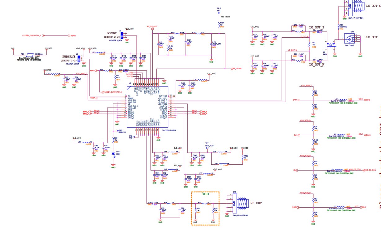
We are working with TRF372017 IQ modulator on our custom board and are currently trying to program the seven registers in it for a modulated output of 2450 MHz. Looking at the modulator's data sheet, we expect, for a divider value of 2 from VCO output to RF mixers input and divider value of 1 from VCO output to the tap provided, we should see 4900 MHz at the VCO tap output. Our reference clock is 30 MHz and can be changed, if required. Following is the schematic for reference.

Can someone suggest what is the sequence in which the registers need to be programmed and what are the optimized values for all seven registers, to obtain modulated output of 2450 MHz?

Also, what are the status registers available and how to read their values? For example, the PLL lock status? If someone can respond, that would be helpful too.

-Chan100

  • Hello Chan100,

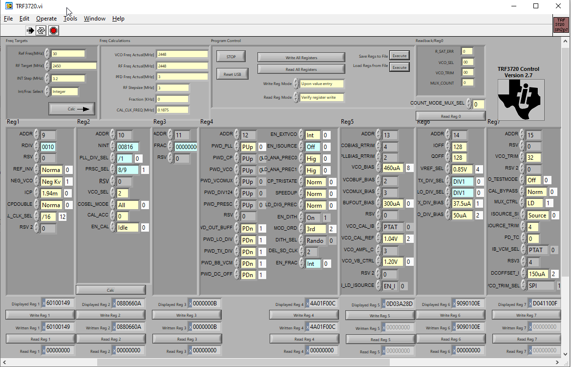
    You may download the TRF372017 EVM GUI and dump out the sequence after the GUI calculation for the register settings.

    The value of sequence depends on integer or fractional mode

    All status registers are available on the TRF372017 datasheet, section 7.5.1.2

  • Hello,

         We do not have an eval board which will allow us to tap and obtain the programming sequence. Please advise on what can be done in this case.

    Also, how to determine the optimal loop filter values.

    Thanks,

  • Hi,

    The software can be used without EVM in simulation mode. Simply calculate the value and press write registers and the new register values will be updated.

    Loop filter values can be calculated with tools below:

    -Kang

  • Hi Kang,

    The reason we are emphasizing on the sequence to follow in programming the registers is, for example, the MSB of register 2 is to be set for VCO calibration. Hence we assume that some of the other registers need to be written to, before we go on and try setting the bit for voltage calibration.  Similarly we assume there might be some other such dependencies for which the order of writing among registers might be important.

    Can you suggest if our assumption is right and provide with the sequence of programming registers? If no, can you provide suitable alternate to our situation?

    Thanks in advance,

    -Chan100

  • Hello Chan100,

    I understand your question now. 

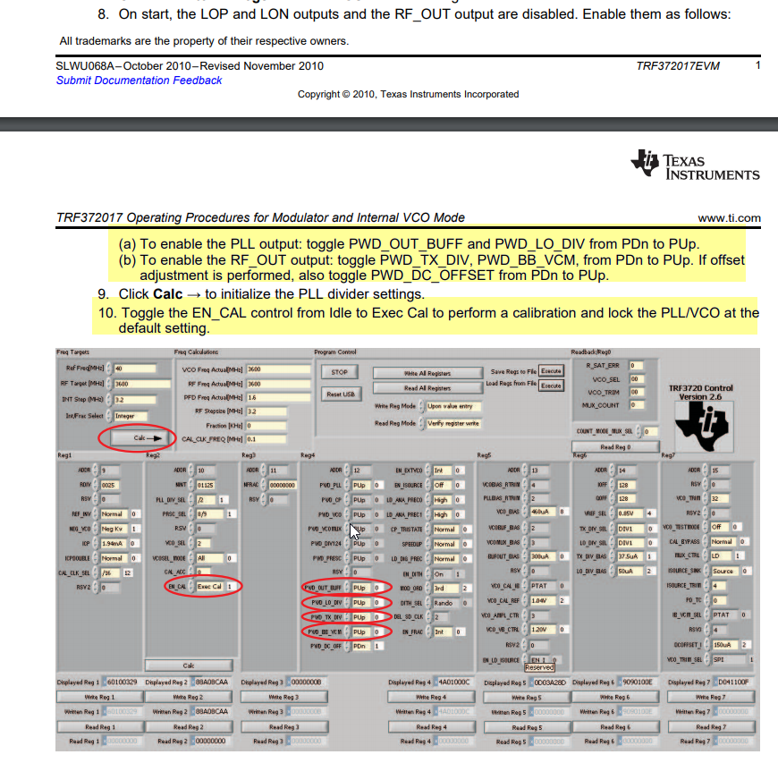
    Based on my usage before on the EVM, upon the completion of the EVM programming, I only have to do the following steps:

    The loading of the registers are linear. The post steps of enabling the RF and LO output, and also calibration, are done separately. Also, the associated register writes for RF/LO output + calibration can be reflected in the register setup display at the bottom of the GUI.

    -Kang

  • Hi Kang,

    Thanks for the reply. We would like to store a configuration into EEPROM and on power cycle, hence read the VCO_BIAS trim settings from it. I see that based on the value of Bit31 of register 7, the configuration settings are either retrieved from EEPROM or is done via SPI. We currently prefer the former case and would like to store the settings on EEPROM. Can you also suggest how we can do that?

    Thanks in advance,

    -Chan100

  • Hi Chan100

    The EEPROM is meant to store some settings from TI factory for the VCO bias. The storage is not meant to store the entire programming sequence of the TRF372017.

    The VCO bias and PLL bias should be programmed as recommended below. Therefore, for this bit 31 of register 7, you should set to SPI writes only

  • Hi Kang,

    Thanks for the reply.

    -Chandrasekhar DVS