This thread has been locked.

If you have a related question, please click the "Ask a related question" button in the top right corner. The newly created question will be automatically linked to this question.

DRV5055: Hall element selection

Part Number: DRV5055

Hi Team,

About temperature compensation and voltage influence

1. Temperature compensation problem

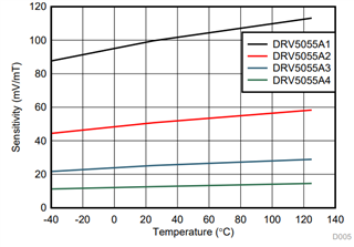
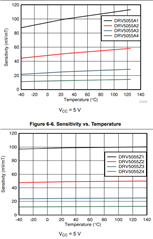
From the curve, the sensitivity of A1 increases with temperature, and the sensitivity of A4 basically does not change. Does this mean that A1 has temperature compensation, but A4 has no temperature compensation?

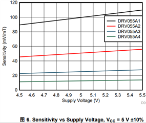
2. Input voltage influence problem:

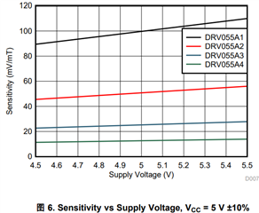
Does this curve show the effect of input voltage on sensitivity? It can be seen that A1 changes greatly with voltage, and A4 basically has no change. Customer would like to know could it be understood that when choosing a Hall chip, he should choose a Hall element such as A4 that has a relatively small voltage fluctuation?

Thanks,

Annie

  • Annie,

    1.  All four devices are actually set to the same temperature compensation 

    The difference in slope has to do with the sensitivity differences of each.  For example, A1 has a sensitivity of 100 mV/mT, so it needs to drift by 0.12 mT/C.  A4, on the other hand, has a sensitivity of 12.5 mV/mT, and so the output will only vary by 0.014 mT/C.  This compensation is to counter the expected -0.12%/C which is typical to NdFeB magnets.

    2. The effect shown on the second plot is related to the "ratiometric" feature of DRV5055.  What happens here is that regardless of the supply voltage, the device will maintain a relatively constant input BL sensing range.

    That is, that with Vcc = 3.3 V or Vcc = 5V, 21-22 mT will produce a full scale output voltage. Using the same Vcc as a full scale reference to a DAC will help produce consistent conversion results regardless of Vcc variations. Again, this slope is related to the Sensitivity and the required changes to maintain this behavior, so we see different behavior from A1-A4.

    Thanks,

    Scott

  • Hi Scott,

    Thanks for your answer.

    1. In the table and curve below, A1 and Z1 have the same sensitivity and BL sensing range, but the slopes of the curves are very different. The curve of Z1 is similar to that of A4. In the table, the sensitivity temperature compensation is 0. Does this mean that the Z1 does not have any temperature compensation?


    2. That is, that with Vcc = 3.3 V or Vcc = 5V, 21-22 mT will produce a full scale output voltage. Customer would like to know where did you read this 21~22mT? Is it the change of the ordinate in the curve? If it is, then A4 basically does not change.

    Thanks,

    Annie

  • Annie,

    All of the Z1-Z4 package variations are trimmed to have a ~0 mT/C temperature compensation.  A4 does have the 0.12%/C drift, but this represents a small upward trend, where Z4 would be totally flat.  The goal with the zero tempco devices is to allow the customer to account for this in their system as only NdFeB type magnets will drift by this value.  Additionally, if either the magnet or sensor is not exposed to the temperature stress, then the normal temperature compensation will not be correct.  In these conditions it would be recommended to use the Z version of the device.

    For the second question, please refer to the BL specification.  I was citing the A1 version of the device where BL is 21 mT for 5V and 22 mT for 3.3V.  BL can be determined by examining the linear output range of the device and then calculating the required input at the specified voltage required to drive to this maximum value.  So, by adjusting the sensitivity with respect to the supply voltage, the ratio of the output voltage to the full scale voltage should remain relatively constant.

    Thanks,

    Scott

  • Hi Scott,

    The sensitivity of A1 varies greatly within the range of +/-10% of the input voltage. Customer would like to know when designing the circuit, is it necessary to design a special voltage regulator circuit to stabilize the input voltage at a certain value?

    Thanks,

    Annie

  • The idea here is that they would only need to add regulation to Vcc if the reference voltage of the DAC is well regulated and DRV5055 is not.  If the DAC is also using the same unregulated Vcc as the reference voltage, then the shift in the sensitivity will help maintain a constant %FS output level from DRV5055.  With a constant %FS output fed into the DAC.  This makes the output of the DAC more reliable across voltage droop or battery voltage decay.

    An added benefit here is that it helps maximize the SNR of the device by using the maximum value of Vcc allowable.  The best SNR is achieved with the 5V supply, but always requiring a 5V input may be too restrictive, and would prevent applications where only 3.3V is available. The ratiometric response allows the user to select Vcc to suit their system design, keeping in mind that the impact of noise will be lower at higher supply voltages.