This thread has been locked.

If you have a related question, please click the "Ask a related question" button in the top right corner. The newly created question will be automatically linked to this question.

AWR6843ISK: Purpose of Load switch for delaying 3.3V to xWR6843

Part Number: AWR6843ISK

Hi Ti

There's a question that customer wants to clarify.

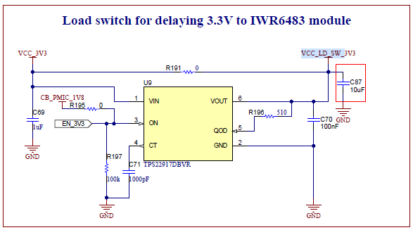
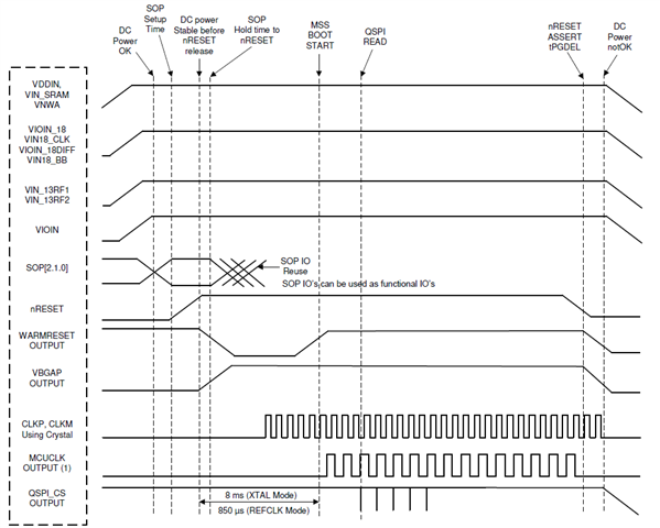
Could you please let us know why we need the load switch circuit for delaying 3.3V.

Are you just trying to comply with the Power Up sequence especially for VIOIN ramping timing?

Thanks.

Regards, 
Jack

  • Hello Jack, 

    I've forwarded your concern to a hardware expert. Please expect a response before the end of this week. 

    Regards,

    Ishita

  • Hi Ishita,

    One more thing, I'd like to ask you about the min. and max. timing specification for delaying VIOIN(3.3V) to xWR6843. Please let me know.

    Regards,

  • Hello Jack,

    The load switch is designed to delay the AWR 3.3V supply from coming up until after the AWR 1.8V supply. If the AWR 3.3V supply comes up first, this can create a glitch on the MMIC GPIO pins.

    There is one error in the schematic. The NRST should also be delayed by the load switch. This needs to be fixed in a future revision. In the current schematic, the NRST is not connected to the load switch output, which is incorrect as this violates the timing diagram you have provided above. NRST should only come up after the MMIC supplies are stable.

    There is no min/max timing for the delay of the 3.3V supply. It can come up anytime relative to the other MMIC supplies and it will not cause any damage to the device, but you may see a glitch as mentioned above if it comes up before the 1.8V supply. The only requirement is that all supplies are stable for a few milliseconds before NRST is released. 

    Regards,

    Adrian