Other Parts Discussed in Thread: USB2ANY,
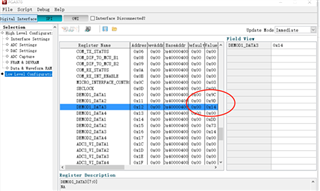
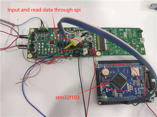
1)I use STM32F103 to send and read data through SPI.
This is a record of the data.
970_Power
01,80,00 => 05,00,00
01,80,00 => 05,00,00
4C,C0,00 => 05,00,00
4C,C0,00 => 05,00,00
970_SPI
40,C0,00 => 05,00,00
40,C0,00 => 05,00,00
01,90,30 => 05,00,00
01,90,30 => 05,00,00
40,D0,00 => 05,00,00
40,D0,10 => 05,00,00
01,80,00 => 05,00,00
01,80,00 => 05,03,00
970_Vref_en
4A,10,00 => 05,03,00
4A,10,40 => 05,03,00
970_sigma delta
4A,10,00 => 05,03,00
4A,10,40 => 05,03,00
44,90,20 => 05,03,00
44,90,00 => 05,03,00
44,10,10 => 05,03,00
4C,F0,20 => 05,03,00
44,90,80 => 05,03,00
45,30,40 => 05,03,00
47,98,20 => 05,03,00
47,98,20 => 05,03,00
970_center freq
53,10,00 => 05,03,00
53,30,00 => 05,03,00
53,50,00 => 05,03,00
53,90,00 => 05,03,00
53,B0,00 => 05,03,00
53,D0,00 => 05,03,00
54,10,00 => 05,03,00
54,30,00 => 05,03,00
54,50,00 => 05,03,00
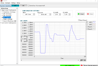
2)
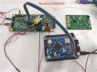
When USB2ANY is removed, all other configurations remain unchanged.
The data was different from the previous comparison. The data collected the second time was not consistent with my expectation, but I could not find the problem
This is a record of the data.
970_Power
01,80,00 => 05,00,00
01,80,00 => 05,00,00
4C,C0,00 => 05,00,00
4C,C0,00 => 05,00,00
970_SPI
40,C0,00 => 05,00,00
40,C0,00 => 05,00,00
01,90,30 => 05,00,00
01,90,30 => 05,00,00
40,D0,00 => 05,00,00
40,D0,10 => 05,00,00
01,80,00 => 05,00,00
01,80,00 => 05,03,00
970_Vref_en
4A,10,00 => 05,03,00
4A,10,40 => 05,03,00
970_sigma delta
4A,10,00 => 05,03,00
4A,10,40 => 05,03,00
44,90,20 => 05,03,00
44,90,00 => 05,03,00
44,10,10 => 05,03,00
4C,F0,20 => 05,03,00
44,90,80 => 05,03,00
45,30,40 => 05,22,81
47,98,20 => 45,00,04
47,98,20 => 05,00,04
970_center freq
53,10,00 => 05,22,80
53,30,00 => 45,22,CA
53,50,00 => 45,22,CA
53,90,00 => 45,00,00
53,B0,00 => 05,00,00
53,D0,00 => 05,00,00
54,10,00 => 05,00,00
54,30,00 => 05,00,00
54,50,00 => 05,00,00
3)
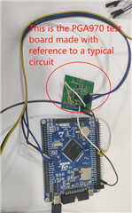
In the third test, there was no change except that the test board of PGA970 was changed, but the data collected was completely inconsistent with expectations. This phenomenon puzzles me.
This is a record of the data.
970_Power
01,80,00 => 00,40,00
01,80,00 => 00,40,00
4C,C0,00 => 00,00,00
4C,C0,00 => 00,00,00
970_SPI
40,C0,00 => 00,00,00
40,C0,00 => 00,00,00
01,90,30 => 00,40,00
01,90,30 => 00,40,00
40,D0,00 => 00,00,00
40,D0,10 => 00,00,00
01,80,00 => 00,40,00
01,80,00 => 00,40,00
970_Vref_en
4A,10,00 => 04,00,00
4A,10,40 => 04,00,00
970_sigma delta
4A,10,00 => 04,00,00
4A,10,40 => 04,00,00
44,90,20 => 00,40,10
44,90,00 => 00,40,00
44,10,10 => 00,00,00
4C,F0,20 => 00,00,10
44,90,80 => 00,40,40
45,30,40 => 00,00,00
47,98,20 => 00,44,10
47,98,20 => 00,44,10