Other Parts Discussed in Thread: AWR6843, IWR6843ISK
Hi TI
There's a question that Customer wants to clarify.
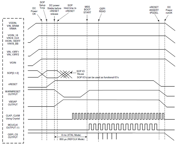
The following timing diagram is for AWR6843. There's no specific timing values to be followed obviously.
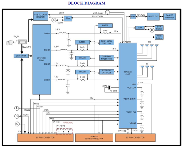
According to EVM schematic, LP87524J PMIC was applied as below.
We want to know the LP87524J comply with AWR6843' wake up sequence below without the customized OTP (or NVM) programming for AWR6843.
Should the OTP with the relevant output timing of each DCDC be used along with customized OTP for AWR6843?
If Not, Did you design only the VIOIN by adding a delay through the Load Switch along with LP87524J's factory default output?