Hello,
I am planning to make an array of sensors (10-15) on a PCB substrate. I have two queries with respect to shielding and multiplexing. I am relatively new to this. So kindly bear with me.
For example, say, 3 devices (senor-ground combination) on a PCB substrate.
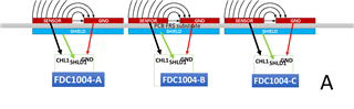
Option A-
- 3 FDCs- A, B and C
- connect CHl1, SHLd1 and GND of A, B and C, connected to devices A, B and C, respectively.
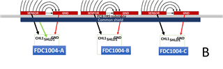
Option B-
- Use 3 FDCs- A, B and C
- FDC-A, B and C, connected to Chl1 and Gnd of devices A, B and C, respectively.
- FDC-A SHLD1 acts as a common shield for devices A, B and C
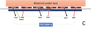
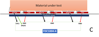
Option C-
- 1 FDC-A-
- device A-CHL1 and GND
- Device B CHL2 and GND
- Device C- CHL3 and GND
- Common shield SHLD1
My queries are as follows:
1) with respect to shielding, does option B works the same as option A? devices B and C are driven by the shield of A. Is this practical?
2) Are the connections for option C correct if I plan to use the 3 channels from the same FDC (e.g. A) ? Also, how to resolve the different baselines of each channel? All my individual sensor channels have the same dimensions. I plan to monitor the sensor output for 4 different locations of my material under test, which is uniform.
it would be great if someone could explain this to me. Would highly appreciate this.
Thanks
Hari