This thread has been locked.

If you have a related question, please click the "Ask a related question" button in the top right corner. The newly created question will be automatically linked to this question.

IWR1443: self-developed board dB value lower than IWR1443Boost

Part Number: IWR1443

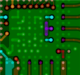
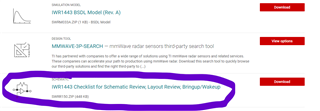
Hardware: PCB designed by ourselves with IWR1443 reference to IWR1443Boost.

Software: xwr14xx_mmw_demo.bin + mmwave demo visualizer 2.1.

Test environment: IWR1443 board face to the ceiling, about 2.5 meters. 

Everything works fine.

IWR1443Boost can get about 113dB at 2.5 meters, but our PCB board can only get 90dB.

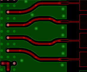
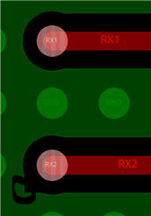
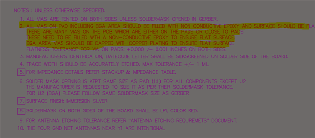
Please check our PCB files by Cadence 16.6 and give us some advices.

IWR1443Ant-V1.brd

  • Hello,

       Could you please provide the  stackup used for the PCB construction and schematic as well? 

    Thanks and regards,

    CHETHAN KUMAR Y.B.

  • Hello,

       Thank you for sharing the schematics. Could you please share the stack-up used for the PCB. 

    I'm assuming you are using R04835lopro 4mil substrate for the Antenna layer. 

    Below are the few feedback from the schematics

    1) If you are using 1V for the RF supply then it's recommended to connect R41 always.

    2) Power supply details are not shown,  It's important meet the Ripple/Noise requirements as per the data sheet needs. 

    3)  Crystal capacitors and resistors:

    For the crystal 4.7pf capacitors are recommended,  schematic shows 10pf which is much larger than recommended.

    R23 resistor need to be removed, this disturbs the biasing & loads of the oscillators. 

    Bigger problem is seen with the layout:

    1) Layout requires mico vias for the RF traces (These are GCPW 50 ohm traces) which is missing in the layout.

    Micro vias are needed around the RF balls and via fencing for the RF trace, Without this transmission line will not be matched to RF Ball or Antenna ports. This is the most important issue in the design which is causing poor output power and link-budget.

    Please refer to IWR1443BOOST EVM reference design

    also for the Rx2 shown below on the top layer ground clearance is not proper these kind of structure causes impedance mismatch.

    Just under the RF balls there are ground opening are provided as impedance matching structures, They are missing in the current layout.

    Please refer to schematic and layout checklist for the board development before sending it to fabrication. 

    https://www.ti.com/lit/zip/swrr150

    Thanks and regards,

    CHETHAN KUMAR Y.B.

  • Thank you for your reply. Really helpful for us. 

    1) Layout requires mico vias for the RF traces

    We checked the IWR1443Boost board, there are no mico vias on board in spite of he mico vias marked on sprr253-IWR1443BOOST Layout and Design Files.

    2)Just under the RF balls there are ground opening are provided as impedance matching structures, They are missing in the current layout.

    We don't understand about it. We have the ground layout. Please check again.

  • Hello user1213293 ,

         Please see below screenshot of the reference design which shows the micro vias in the design. Micro via must be needed to ensure 50Ohm GCPW transmission line.

    Please review the FAB notes, vias are filled and capped with copper plating to ensure flat surface. If you see through the top surface you will not notice presence of Via. You need to do cross section examination to identify the Micro vias. 

    2) Layer 2 ground opening under the RF balls:

    Please note in the below reference layout of the EVM, there is ground opening provided for the RF signal as impedance matching structures in the Layer2.

    This is mentioned in the above "layout checklist" under Layout guidelines in the checklist. 

    Thanks and regards,

    CHETHAN KUMAR Y.B.

  • Thank you dor your fast reply. Great helpful for us.

    Do you have any other suggestions about the sch and PCB. Could you check again and thanks in advance.

  • Hello,

       Typically E2E forum is not meant to perform schematic and layout reviews.  We encourage to follow the schematic and layout checklist provided in the above link.  

    Thanks and regards,

    CHETHAN KUMAR Y.B.