


This FAQ discusses the Memory Architecture and Allocation of Applications implemented on programmable mmWave sensors.
Programmable mmWave sensors include an ARM core (MSS) and one or both of following processing engines: Hardware Accelerator (HWA) and DSP (DSS).
For Gen1 mmWave sensors the DSP is a C647x, for Gen2 devices the DSP is part of the C66 family.
Following documents include detailed information about the C647x and C66x memory subsystems:
For C647x:
C64x+ Megamodule User Guide
https://www.ti.com/lit/ug/spru871k/spru871k.pdf
For C66
TMS320C66x DSP CorePac
https://www.ti.com/lit/ug/sprugw0c/sprugw0c.pdf
mmWave Sensors usually include following memories:
- L1P, L1D, L2 - DSS memories
- DSS_L3 - shared memory
- Hardware Accelerator Input/Output memories
- MSS_TCMA
- MSS_TCMB - ARM Data memory
In a mmWave Application, the radar processing is usually implemented on the HWA or the DSS.
Memory Allocation for Processing using the HWA
For processing data with the HWA the dedicated Input/Output buffers must be used. There is no alternative.
- Pre-processing the input data is transferred using the EDMA from another memory such as L3 to the HWA input buffer
- Post-processing the result data is transferred using the EDMA from the HWA output buffer to another memory such as L3
To optimize processing input data is organized in PING/PONG buffers. The optimization is due to the fact that processing of the PING buffer happens when the PONG data is transferred by the EDMA. So, there are no additional delays cause by the EDMA transfer of the data. Of course, this optimization requires 2x memory buffers.
A nice example of this type of processing is provided in the mmWave SDK demo documentation for Doppler FFT. See DopplerProcHWA
Doppler DPU
Memory Allocation for Processing using the DSP
When processing data with the DSP, first it is required to have highly optimized implementations of the most cycle intensive algorithms. For best performance fixed point algorithms are desired. If there is need for more precision floating point format may be needed. The DSPs available in the mmWave sensors support both fixed point and floating point data formats. In order for these implementations to provide best performance they have to run from fastest Program and Data memories: L1P and L1D.
Since both memories L1P and L1D can be configured part memory and part cache, the application developer will have the choice to
- use part of the L1P and L1D memory as cache and part as memory.
- use all L1P and L1D as cache
When part of the L1D will be used as memory, the application must allocate in this memory the input and output buffers for the most cycle intensive algorithms. The buffers would be overlayed for each processing stage.
Here is an example from the mmwave SDK 2.1 demo:
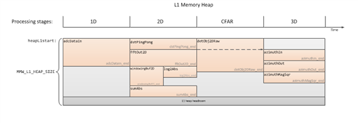
Data would be transferred to and from the L1D buffers using the EDMA. Usually the output results are transferred to L3 memory.
