Other Parts Discussed in Thread: TDC7201, MSP430G2553
Hello, I am trying to configure the TDC1 of TDC7201 on the ZAX EVM Board with STM32F334 controller via SPI protocol.
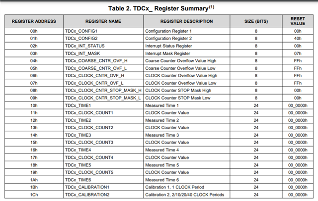
I believe i have configured everything as explained in the Datasheet. I am still receiving 0x00 from the registers i wrote to.
Does anyone have any idea why this is happening?
1) Set Enable PIN.
    // Set the Enable PIN right after power up.
    LL_GPIO_ResetOutputPin(GPIOB, LL_GPIO_PIN_ENABLE);
    LL_mDelay(5);
    LL_GPIO_SetOutputPin(GPIOB, LL_GPIO_PIN_ENABLE);
    LL_mDelay(3);

    //Set the OSC_Enable pin for internal TDC clock.
    LL_GPIO_SetOutputPin(GPIOB, LL_GPIO_PIN_TDC_OSC_ENABLE);
2) SPI CONFIG:
SPI1InitStruct.BaudRate = LL_SPI_BAUDRATEPRESCALER_DIV2;
SPI1InitStruct.ClockPhase = LL_SPI_PHASE_2EDGE;
SPI1InitStruct.ClockPolarity = LL_SPI_POLARITY_LOW;
SPI1InitStruct.CRCCalculation = LL_SPI_CRCCALCULATION_DISABLE;
SPI1InitStruct.DataWidth = LL_SPI_DATAWIDTH_8BIT;
SPI1InitStruct.TransferDirection = LL_SPI_FULL_DUPLEX;
SPI1InitStruct.BitOrder = LL_SPI_MSB_FIRST;
SPI1InitStruct.Mode = LL_SPI_MODE_MASTER;
SPI1InitStruct.NSS = LL_SPI_NSS_SOFT;

LL_SPI_Init(SPI1, &SPI1InitStruct);
LL_SPI_SetRxFIFOThreshold(SPI1, LL_SPI_RX_FIFO_TH_QUARTER);
LL_SPI_Enable(SPI1);
3) Function: Write Register:
 if (!LL_SPI_IsEnabled(SPI1))
    {
        LL_SPI_Enable(SPI1);
    }

    uint8_t  raddr;

    raddr = TDC_WRT_MASK | address; // set addr bits 7 to 0 & 6 to 1 for write.

    LL_GPIO_ResetOutputPin(GPIOA, LL_GPIO_PIN_4); // slave select (low)

    LL_SPI_TransmitData8(SPI1, raddr); // send reg address.
    LL_SPI_TransmitData8(SPI1, value); // send Reg value data.

    while (!LL_SPI_IsActiveFlag_TXE(SPI1))
        ;

    while (LL_SPI_IsActiveFlag_BSY(SPI1))
        ;

    LL_GPIO_SetOutputPin(GPIOA, LL_GPIO_PIN_4); // slave deselect (high)
    LL_SPI_Disable(SPI1);
4) Function: Read Register:
    if (!LL_SPI_IsEnabled(SPI1))
    {
        LL_SPI_Enable(SPI1);
    }

    uint8_t data = 0x00;

    uint8_t raddr;

    raddr = address; // set addr bits 7 & 6 to 0 for read

    LL_GPIO_ResetOutputPin(GPIOA, LL_GPIO_PIN_4); // slave select (low)

    LL_SPI_TransmitData8(SPI1, raddr);

    while (!LL_SPI_IsActiveFlag_TXE(SPI1))
        ; // wait while not empty

    while (LL_SPI_IsActiveFlag_BSY(SPI1))
        ; // wait while busy,

    *(volatile uint8_t*)&SPI1->DR = 0; // dummy write

    while (!LL_SPI_IsActiveFlag_RXNE(SPI1))
        ;

    data = LL_SPI_ReceiveData8(SPI1);

    LL_GPIO_SetOutputPin(GPIOA, LL_GPIO_PIN_4); // slave select (low)

    LL_SPI_Disable(SPI1);

    return data;
When i Write and read after write i am getting 0x00.
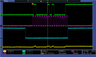
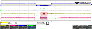
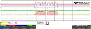
Image 1: Master Out Slave In (MOSI:Green, SCLK: Pink, Chip Select: Blue)
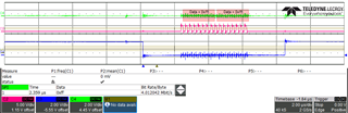
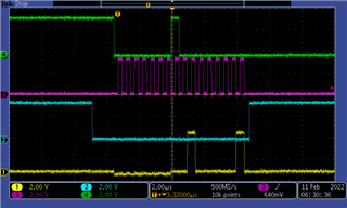
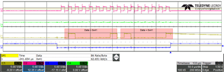
Image 2: Master In Slave Out (MISO:Green, SCLK: Pink, Chip Select: Blue)