


Dear Ladies and Gentlemen,
I am currently searching for a problem I can't wrap my head around. I had the PGA411 working fine on a self-developed PCB for almost a year now. From one day to another, the device started entering FAULT state within a fraction of a second upon initialization. I read back the FAULT flags and was able to identify the FBSTOV flag as the fault origin. Therefore, I setup an oscilloscope measurement for the generated DC voltage. The voltage level is smooth and the switching pattern looks regular, however the output voltage level is not correct. There seems to be a voltage offset of about 3V between the voltage setpoint and the voltage generated:
| Setpoint [V] | Actual Voltage [V] |
| 10 | N/A |
| 11 | N/A |
| 12 | N/A |
| 13 | N/A |
| 14 | 17,4 |
| 15 | 18,3 |
| 16 | 19,1 |
| 17 | 20,0 |
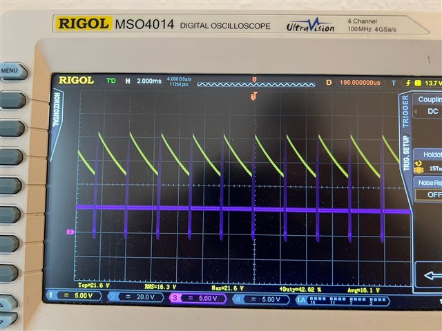
The feed-forward was turned off for this measurement, turning it on resulted in a voltage reduction of approximately 0,3V, both with or without load. For voltage setpoints of 13V and below, the voltage pattern was not smooth anymore, as the integrated switch periodically paused switching for approximately 2,35us. This happened independent of the choice of 7Vrms or 4Vrms excitation. See the oscilloscope shot shown below for a setpoint of 12V:
I checked and resolvered all IC pins and passives for cracked solder joints, but to no avail. Therefore, I would like to ask whether this failure mode is common or at least explicable and whether you have any other suggestions of things I could try. As it worked fine for so long and no software modifications were performed, I doubt this is caused by a bad configuration. As a remark, the data sheet and the trouble shooting guide give inconsistent information about the voltage monitoring that sets FBSTOV: In the trouble shooting guide SLAA687 on page 6, the VEXT pin is stated as the pin in question, the datasheet states it to be VEXTS. A clarification on this would be appreciated. In my opinion, the degree of detail given concerning the boost circuit leaves room for improvement.
Lastly, I a m using this device in a government funded research project and was surprised to find the chip was changed to be a NDA product from one day to the other. As a personal note, I dislike the removal of data on obsolete or changed products, as there may be customers still relying on support for the products they purchased. I would be very pleased if you were to get in touch with me in order to get access to the full documentation as well as the opportunity to order or back-order, as we are already low on stock and would like to avaid having to change the resolver interface on short notice. Thank you in advance!
Yours sincerely,
Steffen F.

