This thread has been locked.

If you have a related question, please click the "Ask a related question" button in the top right corner. The newly created question will be automatically linked to this question.

PGA970: Few questions regarding interfacing PGA970 With LVDT

Part Number: PGA970
Other Parts Discussed in Thread: USB2ANY

Hello,

I am designing a board featuring PGA970 to use it with an LVDT. My required Excitation signal is 3Vrms , 5kHz.I have few questions regarding IC.

1) The DAC range is stated to be 1.25V in the data sheet . is this is peak to peak voltage ? Assuming that the gain = 1 , if I take the excitation signal differentially between P1 and P2 will the signal still be 1.25V p-p or will I be able to reach 2.5V ?

Also at the amplification stage if I use 1.67V/V as gain will I get a differential signal of 2.0875 p-p between P1 and P2 or can I get 4.175V p-p ?

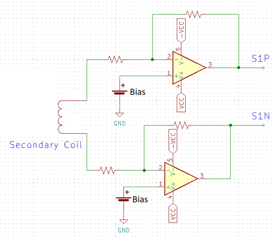
2) Regarding the secondary windings at 3Vrms , my LVDT produces 2.312Vrms which is 3.269V peak. Since the ADC range is 0 to 2.5V (peak to peak I think) , this means that I need to attenuate my signal externally before applying it to S1 and S2 ?

3) For the communication with the IC , I am planning to use SPI or adding the connector that matches the connector of USB2ANY in order to be able to use the GUI.

If the communication has been removed will the IC still works (produces excitation signal and produces DAC output voltage) depending on the stored code even when resetting it or does it need constant communication in order for it to keep operating?

Thank you very much in advance/

BR 

Amr

  • Update (2)

    i Noticed the BIAS_VCM_CTRL in the data sheet which according to my understanding could be useful in biasing the bipolar signal to become unipolar within the acceptable range of the Sp1 and Sp2 PINS 0.05 TO 2V. But I guess I still need to attenuate the differential signal before biasing it so I need your reply on the acceptable input range? Are the 0.05V to 2V Peak to peak value of the differential signal from transformer?

  • Update (1)

    After checking the evaluation board data sheet and many forum questions , my conclusion is that the peak to peak output voltage before amplification is 0.375V and with 1.67 Gain is 0.62625V on each of P1 and P2 so the differential signal betwween P1 and P2 will be 1.2525V p-p so finally I Understand the Primary coil excitation.

    Still trying to figure out the rest two points

  • Hi Amr,

    The relevant requirement for the input signal is the S1 and S2 gain stage input limits, which are a maximum of 2V (single-ended). You will need to make sure the individual single-ended input of each of the S1x and S2x pins are below 2V, which may require some external attenuation. From there, you have noted that the demodulator inputs (the output of the gain stage) needs to be 2.5V peak to peak, so choose your S1/S2 gains accordingly.

    The FRAM program memory is nonvolatile, so once you have stored your firmware in the FRAM it will be saved on powerdown, and start running from the beginning at each powerup.

    Regards,

    Scott

  • Thank you very much for your reply.

    1) Regarding the operation of the PGA970,  the MCU doesn't require any external communication except once and it could store the gain , amplitude and all the configurations that were only once programmed through USB2ANY or XDS2000 ? The board will keep functioning without any kind of external connections except power or am I wrong?


    2)  if I designed my custom board with the IC can I still use the GUI of the evaluation board if I added the same connectors of USB2ANY and XDS2000 on my board? I am planning to use SPI as my communication protocol , Can I connect GPIO_OWI_TX using a pull down resistor to GND and hardwire the SPI MISO , MOSI to SPI_SOMI AND SPI_SIMO of the USB2ANY connector or Do I still need to add the analog switch for proper communication with the GUI ? Also  I gonna float all the OWI pins like GPIO_OWI_ACT , SDA,SCL ,GPIO_OWI_VDD.

    3) Regarding S1 and S2 , Can I go below Zero volts in case I am going to use BIAS_VCM_CTRL to bring the signal internally above zero or should I strictly stick to the 0.05 to 2V range on the pins ? If I need to stick to the 0.05V to 2V range then I need to add common mode externally not just Attenuator (Voltage divider) or am I wrong ?

  • Hi Amr,

    All of the configuration registers for the PGA970 are in volatile memory and will not be stored when the part is powered down. However, the internal M0 microprocessor program memory is stored in nonvolatile FRAM. Typically the firmware you program into the part will have an initialization function that runs at startup and configures all of the registers each time.

    If you only intend to use the SPI interface, then you can leave the other USB2ANY connections floating.

    The internal bias is designed to be used to bring your input within the recommended range. As long as your input (while riding on top of the internal common mode) is within the 0.05 to 2V range, then the part will work as expected.


    Regards,

    Scott

  • Thank you very much for your reply regarding the first 2 points.

    1) For the third point regarding the S1P and S1N inputs , Based on your answer I understood that I need to an external attenuator and also external common mode voltage to shift the signal onto a range from 0.05 to 2V. I think I could use 2 opamps for this purpose in the following configuration. I just need confirmation that it will not affect the input impedance of the IC or anything.

    Note : I am planning to use OPA1656ID from TI.

    2) On the evaluation board there are 47nF capacitor and a 43K resistor that provide decoupling/Attenuation with the internal Resistance of the IC. I think I don't need the 43K Resistor as i already have my signal attenuated but i still need to decouple the signal using the 47nF capacitor? My signal is 5kHz Signal I think the cut off of 47nF is ok for me isn't it ?

    3) Is it ok not to add any circuits related to OWI since I am only interested in communication through SPI ?

    Thank you very much in advance.

  • Hello,

    If you only intend to use SPI, there is no need for the extensive OWI circuitry. Just make sure you put some bypass capacitance on the VDD voltage input according to the application diagrams in the datasheet.

    This setup you have included will work well, and the 47nF capacitor should be fine in this application with a 5khz signal.

    Regards,

    Scott