This thread has been locked.

If you have a related question, please click the "Ask a related question" button in the top right corner. The newly created question will be automatically linked to this question.

FDC1004: source and bandwidth

Part Number: FDC1004

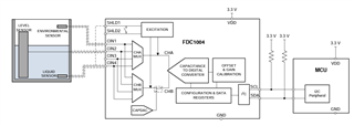
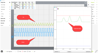
Hello, below in the image is the excitation signal waveform measured on the Cin pin from the FDC1004.

There are a couple of questions:

1). why is the Cin/excitation signal shaped like this (in 2 steps)?

2). are the Cin and excitation signals driven from the same generator or are there 2 generators inside the chip?

3). what is the bandwith of the signal? Or the delta-t of the rising flank of the signal / rising time?

Thanks!

  • Marc,

    The waveform is derived from the analog front-end which is based on a switch-cap buffer that senses the changes in the sensor capacitance and then uses the changes to drive an internal A/D converter.

    There is an internal reference clock, in addition to the 25kHz clock that drives the input buffer.

    We don't really have any readily available specs or data we can share on the sensor signal itself.
    Can you say why this information is important to your application?

    Regards,
    John

  • Hi John, thanks for the reply.
    We need this information /data because we use simulation for a client specific situation.
    Could you please provide us as much information as possible?
    -Is there 1 source for both signal Cin and excitation OR do they have separate sources?
    -Can you provide the rise time or bandwidth of the signal?
    -Why is there between a series of pulse-shapes no signal at all? Is the conductive response measured by the chip here?
    -If possible perhaps a high level description why the signaling is in a 'hat' shape?
    Regards,
  • Marc,

    I looked thru some internal docs and don't see any rise time or BW info on the signal at the device pins.
    The waveform looks the way it does because it is part of a signal chain that consists a switch-cap buffer that outputs narrow, precisely timed pulses that serve as input signals to a conventional  A/D converter. 

    Can you provide more info on the types of sim results you are looking for? We might be able to help with that.

    Also, would a Spice model of the device be useful for what you are doing?
    It would not be based on the actual device internal design, and would most likely support only a limited set of features and parameters, but it could reflect some nominal high-level behaviors. 

    regards,
    John

  • Hi John, thanks for the reply.

    The simulation we use isn't spice simulation, but physical/system simulation to determine the size of the sensor in a specific application. Do you mean you have or can obtain sim results for determining the optimal geometric dimensions of the sensor and shield plane?

    Remaining are:
    -Is there 1 source for both signal Cin and excitation OR do they have separate sources?
    -Why is there between a series of pulse-shapes no signal at all? Is the conductive response measured by the chip here?

    Is there some engineer who could answer the risetime/bandwidth question?
    Thanks,
  • Marc,

    We don't have any design aids for the FDC1004 yet, but it is on our plan for later in the year.

    Could you clarify what you mean by signal Cin and excitation? 

    The pulse shape is a little strange, but it has been optimized to work with realistic sensors and the device's internal signal chain to give the required 16b resolution. There is no signal source - like a buffer output - that outputs the pulse on the pins. The pulse is a consequence of the switch-cap AFE input interacting with the sensor capacitance.  We can say the pulse period is 40us, but the pulse rise & fall times will be at least somewhat dependent on the sensor, which can vary ±15pF. The details are considered IP, so that's about all we can say for now.

    The pulse characteristics haven't been part of our published specs, and since they are only a secondary concern there isn't any readily available data in our usual archives.  I will check with our test engineers to see if they have collected some data and update this thread by the end of the week.

    Regards,
    John

  • Hi John,

    Thanks again for your reply.

    With Cin and excitation, I mean the Capacitive input pin (Cin) and the shield pin (excitation). Are those both driven by the switch-cap you mentioned earlier? I assume this switch-cap is located somewhere in the excitation block which is shown in the datasheet?

    Regards, Marc

  • Marc,

    The SHLD pins have an output buffer/driver that outputs the Cin signal on the shield. 
    For all intents and purposes, the Excitation block also represents the signal that shows up on the Cin pins, but thru paths & connections that are different than for the SHLD pins.

    Regards,
    John

  •  Hi John,
    Does this answers the question, i.e., Cin and SHLD have the same source. Can you confirm/do you agree?
    Thanks, Marc
  • Mark,

    The SHLD and Cin have the same source, but the SHLD pin has a buffered low-impedance output and the Cin does not.

    Regards,
    John