


Hello,
Regarding de MMWCAS-RF-EVM, in the PCB documentation (Rev. E) it is specified that a special etching tolerance is required in the antenna structures:
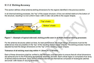
In it, it is specified that the PCB dimensions must be achieved as close as possible on the “top” of the resulting etched copper shapes, contrary to what the PCB manufacturers usually do, where the target dimensions are closer to the "bottom" etch. In fact, the bottom etch width has a stronger effect in the characteristic impedance of the line contrary to the top edge.
What is the desired resulting "bottom" etch in this case? Are we aiming for a standard trapezoidal shape as shown in the image or it is better to have a rectangular one? How much wider should the bottom copper etch be?
Thank you.

