


Hi,
I want to communicate with PGA970EVM using FPGA with spi protocol. I set the MO to reset. I have set S1/S2 GAIN and S1/S2 DEMODULATOR. But I don't know how to write waveform table values to waveform ram while setting WAVEFORM GENERATOR settings.
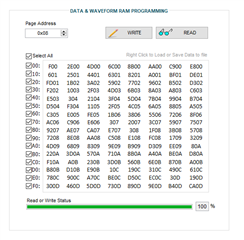
I set the WAVEFORM GENERATION values in the PGA970EVM GUI and created the waveform table shown below. But I don't know how to send the values in this table with spi.
In the datasheet, there is an expression:
"The data and waveform RAM memory can be programmed 1 byte at a time. The upper 4 bits of the 12-bit data and waveform RAM memory address must be loaded into the DATA_WAVE_PAGE_ADDR register. The remaining 8 bits of the data and waveform RAM address are included in the SPI protocol."
An example is given in the Datasheet:
The following sequence is an example to program 0x35 to WAVEFORM RAM memory address 0x1A6 using the SPI digital interface:
1. Write 0x09 to DATA_WAVE_PAGE_ADDR register: 010 00011010 1 00001001 0000
2. Write 0x35 to WAVEFORM RAM address 0xA6: 001 10100110 1 00110101 0000
In this example, the upper 4 bit of 1A6, which is the 12-bit waveform RAM memory address , is not loaded into the DATA_WAVE_PAGE_ADDR register.
Could you write a few lines example of the command lines that will load the values in the waveform table to the waveform RAM with the spi protocol?
Thank you
