This thread has been locked.

If you have a related question, please click the "Ask a related question" button in the top right corner. The newly created question will be automatically linked to this question.

PGA970: Schematic review and suggestions for LVDT excitation and gain

Part Number: PGA970

Hello,

We need to measure a LVDT attached to a hydraulic servo valve and I am not sure what are the proper way to design the excitation and the whole chain conversion.

We have one MCU C2000 connected to the SPI to access all the internal registers and the analog output of the PGA is connected to one ADC input. We just need to read 0-V to 5-V Absolute Output.

The characteristics of the LVDT are as below:

  1. 3V RMS gives 8.5V pk-pk, what value should we choose for VDD?
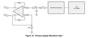
    1. Is it better to keep VDD regulated at 14V using the N-Channel MOSFET, then for the excitation of the LVDT configure correctly the DAC gain (Primary Supply Waveform Gain)+ external amplifier so the EXC signal is in the range 0 - 3V RMS
    2. Or change VDD to a lower value to get more DAC resolution?

  2. What is the initial range voltage of the waveform generator, before the GAIN?
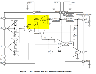
  3. The next step would be to choose the right external resistor divider, filter then GAIN S1,S2 and S3 to have an input range of 2.5V? Is it possible to simulated the whole conversion chain?
  4. In the LVDT datasheet, it says Summed Output Voltage 1.26V/Vin, does it means the transformation ratio is 1.26?
  5. Schematic PGA970.pdf
  • Hi Alexis,

    1. The DAC reference is not affected by the VDD. The 2.5V internal reference is fixed, and cannot be changed, so the DAC reference derived from it will also be fixed. The PGA970 already has a fairly wide VDD supply range (up to 30V), so the external GATE drive is really only needed if it is likely that the supply line might exceed 30V. Otherwise it is not necessary to use the GATE drive. To achieve an LVDT excitation signal of 8.5V peak to peak, you will need to use external amplification.

    2. The waveform generator block is essentially just the waveform DAC output, and the DAC reference is 1.25V.

    3. There is currently no simulation model available for the PGA970.

    4. I would consult the LVDT manufacturer for information on the transformer windings. In any case, with that level of sensitivity, you will need to divide down the output to match the input range of the S1/S2 gain stages.

    5. I will look into the schematic and get back to you.


    Regards,

    Scott

  • Thank you very much Scott,

    Here is the updated schematic without the mosfet. VDD supply is 8V.

    Pretty much the same as the PGA970EVM.
    [4] LVDT PGA970.pdf

  • Scott, can you please confirm we don't need a level shifter for the SPI. Our F28388 is powered with 3V3, and the SPI communication for the PGA use AVDD 3V .

  • Hi Alexis,

    3.3v for SPI will work just fine. This is within the recommended range for SPI signals (AVDD + 0.3V on the high end).

    Regards,

    Scott