This thread has been locked.

If you have a related question, please click the "Ask a related question" button in the top right corner. The newly created question will be automatically linked to this question.

LMP91000: Differential AD converter input at Vout

Part Number: LMP91000
Other Parts Discussed in Thread: THS4551, OPA625, ADS8910B

Hi, 

I'm planning to feed the output to the LMP91000 in 3-Lead Amperometric Cell in Potentiostat Configuration into a differential AN+/- input of an A/D converter. Best would be to have access to the internal zero generated by the LMP91000 to be connected to the negative input of the A/D converter. This allows for potentially turn on the A/D PGA, if available, to increase resolution.

Assuming that the pin C1 is a virtual heart, would be an option to connect the signal pair available at C2/C1 pins directly to the AN+/- of a differential A/D converter?

Thank you and best regards.

Marco.

  • Dear Marco - 

    The output of the LMP91000 s intended to be connected to a single ended ADC. Differential is not needed here. Please see diagram on page 26 here for a reference connection diagram. 

    https://www.ti.com/lit/ds/symlink/lmp91000.pdf 

    Additionally, if you want to connect to the ADC you mention above - you could use shielded twisted pair (actual wire or with PCB traces), with ground twisted with output signal from LMP91000 and with the twisted ground wire also grounded to shield on both ends. 

  • Dear Josh, 

    thank you for your feedback.

    I'm thinking to use differential inputs not for reducing noise in the communication wire, but to be able to apply PGA in the AD converter, thus increasing the minimum resolution we're able to achieve. 

    We're measuring very low pollutant concentrations (i.e. in the ppb range) and, even with the max gain we can implement with LMP AFE (350k resistor), our Vout signal swings by several 100s of mVs only above (below) the "internal zero". Feeding the AFE internal zero to the AN- terminal of the A/D converter would be the best way to obtain a differential signals to be amplified by the PGA internal to the A/D converter. 

    An example to better explain the problem: 

    Internal zero set to 50% of 3.3V -> 1.65V

    Max delta Vout at maximum concentration, with 350k gain: +0.3V

    By using a single ended ADC, Vout swings between 1.65V and 1.95V but, using a differential connection, the signal swing would be reduced to 0V to 0.3V. In the latter, we can add an extra gain through the PGA (i.e. x8) to obtain a max swing of 0V to 2.4V, to better use the A/D bits.

    If, for example, we've a 16 bit AD with 2.5V full scale, with a single ended connection our signal is spreaded over 13bits but with a differential connection it would cover the whole 16 bit set.

    Do you think it would be an option to connect pin C1 to the AN- input of the AD converter? Or do you think something wrong in the concept?

    Thank you and best regards,

    Marco.

  • Dear Marco - 

    Which sensor part number are you using?

  • We've several, but mainly alphasense NO2-B43, NO-B4, CO-A3, OX-A431 and other. The problem is not in the sensors, but in the very low concentrations we're working on...

  • Marco - 

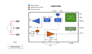
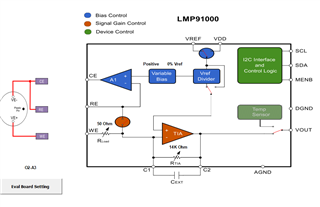
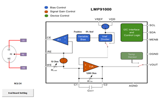
    From looking at the Alphasense datasheets you may want to consider setting up similar to the N0-D4 example, located in the sensor database in the GUI for this device, for the N0-B4. 

    https://www.alphasense.com/wp-content/uploads/2019/09/NO-B4.pdf  vs. https://www.alphasense.com/wp-content/uploads/2020/12/NO-D4.pdf 

    From the same GUI sensor database, the setup for the O2-A3 is provided already: 

    NO2-D4

  • Dear Josh, 

    thank you for the feedback. 

    The settings you suggest where already applied done some time ago (I'm working on a 3rd hw revision of the board). I'm searching for a way to improve the resolution because, in our setup, the concentration of pollutants is very low, and we have a very low output swing at the end of Vout. I'm quite satisfied of the results the LMP91000 provides, but my only concern is related to the way it would be possible to have a differential output, useful to enhance the AD resolution through a PGA. 

    Than you and best regards,

    Marco.

  • Marco - 

    Here perhaps its best to continue using the LMP91000 and your sensors as normal, while amplifying signal going to ADC. 

    For simplest implementation, an amp like the OPA625 coupled with an ADC like the ADS8860 and oversampling/averaging it or filtering with an alpha filter might give you the results you are looking for. (see page 30 of datasheet link) , averaging and alpha filter firmware example can be found here: https://www.ti.com/lit/zip/sboc595 (open either worksheet and then look at Averaging and Low Pass Filter tabs, this was made for an analog temp sensor, but they can be applied to almost anything that needs it)

    If you are still set on using a differential ADC, then you could consider the circuits presented in this TI Precision Lab: https://www.youtube.com/watch?v=HBkQxCvHraU (see around time = 3:35min to around 7:08 for a discrete solution using two OPA625, followed by example using THS4551) both intended to be then sent over to differential ADC (ADS8910B). Might be a good example for you to start with and adjust as you see fit.  

  • Dear Josh, 

    thank you for the feedback and the suggested schematics.

    Moreover, I think it's not the answer to my original question as it moves, but not solves the problem. What I would like to know is if it's possible to use the terminal C1 to intercept the internal zero voltage generated by the LMP91000. If not, is there another option to intercept this value? 

    Than you and best regards,

    Marco.

  • Marco,

      C1 is tied to the WE of the electrode. This is the input from the probe. You can't use it as a reference as this is the probe input and you would always be moving in the VOUT and the reference so the value will always be zero.

    Try setting up an external VREF. This will set the zero for the TIA. Then use the VREF as your differential negative. The VOUT will move with the probe WE input. then you can increase the gain of the TIA to increase the feedback signal level to your differential ADC. 

    If the probe value goes negative then use VREF as the differential positive and the VOUT as negative.

    If the probe is measuring plus and negative values as in a PH value then you can't use VREF as a reference for a differential ADC. You need the zero above ground to swing positive and negative relative to the zero.  

  • Dear Gordon, 

    thank you for your proposal solution. This sounds good to me. 

    I've set the external reference (bit7 set of REFCN) and bypassed the internal zero selection (set 11 to [6:5] of REFCN) and I confirm I can see the VOUT pin swinging from the external VRef I set for the VREF pin. 

    Just a question to clarify some doubts on how the variable bias is implemented. Looking at the figure 25 at page 12 of the datasheet, I see that the "VARIABLE BIAS" block is connected to the "VREF DIVIDER" block. This gives me the idea that the variable bias is referenced by the internal zero voltage, but in the REFCN register explanation I read: "In this condition the Internal Zero and the Bias voltage are defined as a percentage of VREF voltage instead of the supply voltage". 

    I always assumed that the Variable Bias was independent by the Internal Zero... So, if I bypass the internal zero selection, and I use an external Vref, the bias will always be generated from the external VREF voltage present at the Vref pin?

    Thank you and best regards,

    Marco.

  • Marco,

      I should have pointed out that the internal divider for zero will need to be bypassed. This will place the VREF voltage directly on the TIA providing you with a new zero. You will not be able to use VDD as the reference voltage. You will need so place a stable VREF at a lower voltage. Example: use a precision voltage reference of 1.08V then you will have plenty of room to gain up the TIA to increase the dynamic range of your sensor. However, remember that a sudden high concentration can saturate the TIA. It wont hurt the part but it could stay in saturation for an extended time 2 - 4 times your normal sample period before the part will provide a valid new measurement. 

  • Hi Gordon, 

    thank you for your explanation.

    Still the VARIABLE BIAS block do work independently by the internal zero voltage generation? So, if I select the external voltage as reference, and I bypass the internal divider for zero, do the bias voltage still be generated as a percentage from the external voltage reference?

    Thank you and best regards,

    Marco.