Dear TI-Support Team,
I decided to use the DRV5032 Hall effect Sensor in the T0-92 Package because this package can allow me to simplify my PCB design, however from my understanding there are some unclear information provided in the current datasheet you provide regarding this package. Current Datasheet:
https://www.ti.com/lit/ds/symlink/drv5032.pdf?ts=1665084182124&ref_url=https%253A%252F%252Fwww.google.de%252F
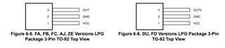
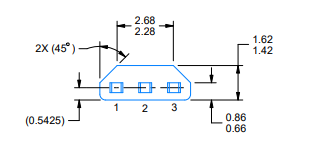
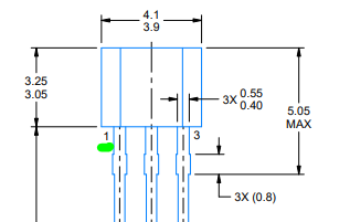
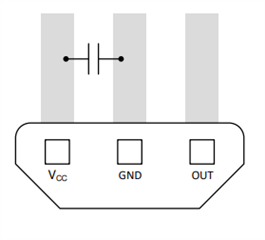
On page 22 (paragraph 11 - Layout) the device in the TO-92 package is shown in a sketch, from what I "guess" is a top down view with the hidden body edges of the leads shown from the top view, as if the plastic cap was transparent. However, in the technical drawings (page 38) the same drawing occurs on the bottom left side of the page, with the same pin assignment from 1-left to 3-right, but the package outline is inverted. Since there is no reference in any of your technical drawings, which projection method you are using according to ISO-5456, I have to assume you are using method 3. This would lead to the conclusion that in Page 38 the device is shown in a bottom view in the lower left side of the page. Can you confirm my assumptions about the views provided on those pages or update the datasheet with a notion on the pages which view-direction is present in the respective drawing (view from top or bottom)?
Best regards
Philipp C.