This thread has been locked.

If you have a related question, please click the "Ask a related question" button in the top right corner. The newly created question will be automatically linked to this question.

LDC1614: I2C gaps between register readings and repeated start to access additional registers

Part Number: LDC1614

Hello,

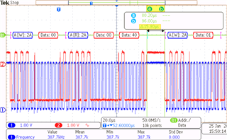
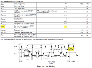
1) Looking at the I2C communication on the evaluation board LDC1614EVM shows a ~16us gap between the Register 0x00 (DATA0_MSB) and Register 0x01 (DATA0_LSB) readings. Is this a limitation of the LDC1614EVM since the LDC1614 specifies only 1.3us?
  

2) Does each register require the five frames of I2C readings shown in "Figure 12. I2C Read Register Sequence" or can the "repeated start" be used as in the way the 2nd byte of each register is read? 
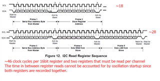
3) I'm trying to figure out the absolute fastest way to read a single channel or two channels and it appears to be ~231us theoretically (~255us in practice) per channel at 400kHz I2C clock and t_BUF=1us. Is that correct?

4) Am I miss-reading the LDC161x datasheet or does it use the terms "MSB" and "LSB" to refer both to the bytes within each 16bit register as well as to the two data registers within each channel? In other words, each register DATAx_MSB is made up of MSB + LSB and each register DATAx_LSB is also made up of MSB + LSB. Is that correct, and if so, could you please inform the authors that this confusing? 

Thank you,

Andrey

  • Hello Andrey, 

    1. The 1.3us is the minimum time required by the I2C bus. The 16us gap is just how the MCU on the EVM is communicating to the device. This time could be cut down if needed as long as it still meets the 1.3us. 
    2. Yes, each register requires the five frames of I2C reading. Repeated start is not supported to read subsequent register addresses for this device. 
    3. The timing for a single register read would be 9 clock frames * 5 I2C frames + setup/hold time for the start and buffers. This should be around 130us for a 400kHz clock. Needing to red two registers would double the transaction time plus a few us for a buffer between them. 
    4. Since the LDC1614 has 16 bit long register data, each I2C transaction breaks that into two 8 bit packets to send to the MCU. When done so, each register read has an MSB and LSB portion. In addition to this, the data from this device is longer than 16 bits so it is broken into two different 16 bit registers and referred to as an MSB and LSB portion. So yes, depending on the context you are looking at, you will see a reuse of the MSB and LSB terms. I hope this helps clear up the confusion and your feedback on this has been noted. 

    Best Regards, 
    Justin Beigel

  • Thank you for the fast response Justin!