This thread has been locked.

If you have a related question, please click the "Ask a related question" button in the top right corner. The newly created question will be automatically linked to this question.

IWRL6432: Questions about PCB single-sided process

Part Number: IWRL6432

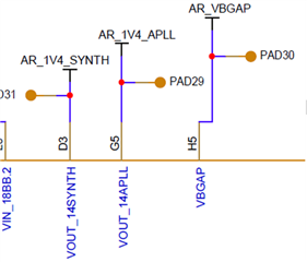
We want to design a single board, so we need to move the IWRL6432 bypass capacitors to the same layer as the SoC.

May I ask, are there any requirements for the bypass capacitors of the following 3 groups(14SYNTH14APLLVBGAP) of power supplies for the IWRL6432 in terms of layout placement, trace routing or impedance?

  • Hello,

    We caps should be placed as close to the pin as possible and trace routing should be kept as short as possible. Avoid any stubs on these traces (i.e. due to test points as in your schematic). L2 below the radar should be a solid GND pour and each cap should have a GND via placed next to the GND pad to provide a short path to the L2 GND. Each of the device GND balls should also have nearby GND via to L2 GND. The main idea is to just keep the total loop from device pin through the cap to the device GND as short as possible. The traces do not need to be routed as controlled impedance traces.

    Regards,

    Adrian