This thread has been locked.

If you have a related question, please click the "Ask a related question" button in the top right corner. The newly created question will be automatically linked to this question.

DRV401: Some confused questions in DRV401 datasheet

Part Number: DRV401

Hi E2E experts,

I'm going to measure 300mA Ipn residual current, with better than 1% zero offset current. I saw some products manufactured by European companies, It seems they are using DRV401 inside.

When reading datasheet of DRV401, I'm confused in the description of compensation loop in page3:

My questions are:

1. What does the COMPENSATION LOOP mean? are the specifications here measured using closed loop with probe and compensation coil? or they are only the specifications of the integrator and filter stages?

2. The 0.03% offset error: does this mean when primary side current is zero, the PWM duty cycle may vary from (50-0.03)% to (50+0.03)%? Is this measured in PWM pin? or it is actualy measured from the feedback current in closed loop back-calculated to a equivalent duty cycle?

3. Does the offset=0.03% mean I can get 0.03% zero offset current? for example: when measuring 300mA current, the zero offset current will be 0.03%*300mA=90uA?

4-1. About the Gain: what does the 25ppm/V Gain mean? does this mean (duty cycle from 50%)/(coil driver differential voltage)?

4-2. About the Gain: what does the |VICOMP1|-|VICOMP2| mean? it seems VICOMP1 and VICOMP2 all are positive voltage (the absolute value of a positive value is itself), do you indeed mean |VICOMP1-VICOMP2|? 

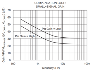
5-1. About the Y-axel label in figure below (in page9 of specification sheet): what does VPMW_AVERAGE mean? what does  (VICOMP1, VICOMP2) mean ?

5-2. Also about the figure as below, it seems the Y-axel label should be  (VICOMP1, VICOMP2) / VPMW_AVERAGE? am I correct?
Looking forward for your reply. Thank you very much!

Yours sincerely,

A_M

  • Hello A_M

    1. What does the COMPENSATION LOOP mean? are the specifications here measured using closed loop with probe and compensation coil? or they are only the specifications of the integrator and filter stages?

    It is the full closed loop with the probe giving a 250kHz PWM signal.  It will include all the integrator and filter compensation and coil in the system.

    2. The 0.03% offset error: does this mean when primary side current is zero, the PWM duty cycle may vary from (50-0.03)% to (50+0.03)%? Is this measured in PWM pin? or it is actually measured from the feedback current in closed loop back-calculated to a equivalent duty cycle?

    I assume this is measured with the PWM signal.  As this is the deviation from 50% of the PWM signal.  I can confirm this but I am confident this is the case.

    3. Does the offset=0.03% mean I can get 0.03% zero offset current? for example: when measuring 300mA current, the zero offset current will be 0.03%*300mA=90uA?

    This is only one part of the offset as this only accounts for the offset due to the PWM not being at 50%.  All the other items in the loop need to be accounted for as well for the offset.

    4-1. About the Gain: what does the 25ppm/V Gain mean? does this mean (duty cycle from 50%)/(coil driver differential voltage)?

    You are correct this is the change of gain vs the change in the coil driver voltage.  So this will change based on your load on the compensation.

    4-2. About the Gain: what does the |VICOMP1|-|VICOMP2| mean? it seems VICOMP1 and VICOMP2 all are positive voltage (the absolute value of a positive value is itself), do you indeed mean |VICOMP1-VICOMP2|? 

    I believe they wanted to express the voltage can vary from -4.2V to 4.2V.  which is an 8.4V range.  I think that is the main thing to consider with this.

    5-1. About the Y-axel label in figure below (in page9 of specification sheet): what does VPMW_AVERAGE mean? what does  (VICOMP1, VICOMP2) mean ?

    This is the gain from the PWM signal to the compensation coil.  The PWM signal coming from the sensor being excited and changed by primary current.

    5-2. Also about the figure as below, it seems the Y-axel label should be  (VICOMP1, VICOMP2) / VPMW_AVERAGE? am I correct?

    I think you are correct as the output is the Icomp pins.

  • Hello Javier sir,

    Great thanks! your reply made me much clear now.

    I am trying to build up a model in my mind according to your explain, to compare with an amplifier circuit which I am more familiar:

    Do you think this model is correct? If my understanding is correct. there still exsits some questions:

    (1) It seems I can measure the offset duty cycle at point B (as the right of the figure shows). because if I measure the duty offset at point A, my oscilloscope need high resolution. 250kHz probe oscillating means 4us cycle time, and 0.03% offset means (4us*50%*0.03%) = 600ps time resolution! 

    (2) If I can measure offset voltage at point B (the differential voltage between Vicomp+ and Vicomp-), then I can calculate the point A offset duty by using the 25ppm/V gain. Do you think this is OK?

    (3) However, according to datasheet(figure as below):

    The gain varies large.  Even there exists -200ppm/V gain. This is strange, I can understand 25ppm/V and 200ppm/V, but the -200ppm/V means the output will be inverted! How to understand this?

    I find there is a figure about the gain (page 9 in datasheet) as below. It varies from -200ppm/V to 200ppm/V,but the title of this figure is DC GAIN: DUTY ERROR CHANGE, and the mean of the histography is 0ppm, not 25ppm. Is this figure means the gain as above? 

    Can you please help reply my questions in bold red font? Since not familiar with DRV401, so many questions are asked here. Sorry to trouble you a lot. 

    Thank you very much!

    A_M

  • Hello A_M,

    I will get to this tomorrow.

  • Hello Javier sir,

    Excuse me for troubling you. Do you have an answer to the questions? 

    Thank you!

    A_M

  • Hello A_M,

    Please understand some of the numbers are based on the 250kHz probe oscillating and will change depending on your probe values.

    (1) It seems I can measure the offset duty cycle at point B (as the right of the figure shows). because if I measure the duty offset at point A, my oscilloscope need high resolution. 250kHz probe oscillating means 4us cycle time, and 0.03% offset means (4us*50%*0.03%) = 600ps time resolution! 

    Yes this is correct and is similar to offset of an amplifier.   This is only one portion of the error.

    (2) If I can measure offset voltage at point B (the differential voltage between Vicomp+ and Vicomp-), then I can calculate the point A offset duty by using the 25ppm/V gain. Do you think this is OK?

    This would be the offset of duty cycle from the original but the change will be from 50% and should not change much.  This would be kind off like CMRR of an amplifier.  But this should be output referenced.  

    The gain varies large.  Even there exists -200ppm/V gain. This is strange, I can understand 25ppm/V and 200ppm/V, but the -200ppm/V means the output will be inverted! How to understand this?

    This is the gain change from the original value and can change in both positive and negative not the gain itself but the delta.

    I find there is a figure about the gain (page 9 in datasheet) as below. It varies from -200ppm/V to 200ppm/V,but the title of this figure is DC GAIN: DUTY ERROR CHANGE, and the mean of the histography is 0ppm, not 25ppm. Is this figure means the gain as above? 

    Out typical values are normally a 1 sigma representation for numbers that are +/- like this value.  For amplifiers even though we average about 0 that number does not make sense as a typical number so we place the 1 sigma.  You can see the distribution is mostly in the +/- 25ppm/V.

  • Hello Javier Sir,

    Great thanks! Much more clear now.

    Yours Sincerely, 

    A_M