Because of the Thanksgiving holiday in the U.S., TI E2E™ design support forum responses may be delayed from November 25 through December 2. Thank you for your patience.

This thread has been locked.

If you have a related question, please click the "Ask a related question" button in the top right corner. The newly created question will be automatically linked to this question.

AWR2944: lvds interface timing sequence

Part Number: AWR2944

We are acquiring raw data of 2944 (in legacy LVDS mode): 1 lvds_clk , 1 lvds_frclk, 2 lvds_tx( i.e. lvds tx0 and lvds_tx1).

We are not sure how data bit is transferred on tx0 and tx1.

For example, data0 and data1 are sent out ( both data0 and data1 are 8-bit):

1)Which bits are sent on tx0, and which are on tx1? (MSB first)

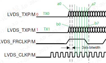
   As shown in the image attached, bit a0~a7 on tx0, bit b0~b7 on tx1, how these 16 bits are combined to 2 bytes?

2) Is the first bit sent at the rising edge of lvds_clk, or falling edge of lvds_clk?

3) Is the first bit sent out when lvds_frclk = 1?

Could you please give us a timing diagram about lvds_clk, lvs_frclk, and lvds_tx0&1?

  • I mean in the TI default SDK, how to configure the data arrangement?

  • Hey Wang,

    Please find my answers below (in bold):

    1)Which bits are sent on tx0, and which are on tx1? (MSB first): It depends on what you configure CFG_LVDS_GEN_x register (Bit 23). You can program it to MSB first/LSB first. The data can be in 12-bit, 14-bit and 16-bit format. Each TXP/M lane will transfer 12/14/16 bits for one Frame_Clock.

    2) Is the first bit sent at the rising edge of lvds_clk, or falling edge of lvds_clk? – First data bit can be sent on either edge of the lvds_clock. It can be changed in the CFG_LVDS_GEN_x register (Bit 22).

    3) Is the first bit sent out when lvds_frclk = 1? Data is sent out when the frame clock is high.

    4) The timing diagram is as below:

    This is similar to the diagram you shared. Can you elaborate on the diagram you require?

    5) How to configure the data arrangement?: You can configure the data arrangement by modifying the values in the CBUFF configuration registers. For more information on the registers, please refer to: https://www.ti.com/lit/ug/spruiv5a/spruiv5a.pdf (Section 23.2 and 23.3).

    Regards,

    Swati