This thread has been locked.

If you have a related question, please click the "Ask a related question" button in the top right corner. The newly created question will be automatically linked to this question.

PGA900: OWI issue with put a MOESET (BSS169) on the VDD pin

Part Number: PGA900

Hello,

We are developing pressure transmitter with your PGA900, we got some issues for OWI communication (and for calibrations) can you please help.

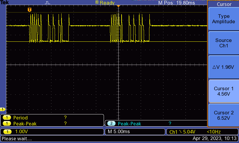
We can do ratio-voltage output model with OWI calibrations without add a MOSFET(BSS169) on the VDD pin, but when design 4-20mA current output that w added a MOSFET (BSS169) on VDD pin as picture below, then we cant communicate PGA900 via OWI, if we removed the MOSFET and shorten the circuit between MOSFET D and S pin, OWI communication is running well.

We guess this could be the VDD has been fixed to 3.5V by the MOSFET while we use 4.8Vfor the OWI_VIH and 4.2V for OWI_VIL as per PGA900 datasheet, can you please advise what settings (or how) we should do to enable OWI communications while we added the MOSFET on the VDD pin? Thank you!


Tomy

  • Hi Tomy,

    Let me take a look and get back to you towards the end of the week.

    Thanks,

    -Cole

  • Hi Tomy,

    Still working on it. Just thought I'd check in.

    Best,

    -Cole

  • Hi Tomy,

    Please provide screen shots that show your OWI activation pulse and the OWI communication, essentially what you see in Figure 29.

  • Hi Tom,

    Please see the pictures as below, supply voltage 18V.

    With our settings, we measurred the voltage at VDD pin is 3.7V, is it correct? If not, how we can set to make a right voltage at VDD pin?

    Thanks!

  • Hi Tomy,

    It looks like those voltage spikes on the rising edge could be causing the issue. Can we increase the capacitance on the node to smooth it out? In addition, are they spikes present when you bypass the FET?

    Best,

    -Cole

  • Hi Cole,

    Sorry, the pictures sent to you days ago was the OWI signal before FET, after FET, there is no singal output, please see picture below (blue), I think this is because the voltage has been fixed to 3.7V at VDD pin after FET , we can't find in the datasheet where we can adjust the gate voltage to enable the VDD pin to be more than 10 V after FET, can  you please check what settings we can adjust to enable the OWI communication with the FET (at least the OWI singal before and after FET should be same shapes).

    Thank you!

  • Hi Tomy,

    Oh I understand the problem now, I apologize.

    The GATE pin's purpose is to regulate the voltage down around 3.5V, you have to disabled the regulation feature (and put the MOSFET into the saturation region) when you want to communicate with OWI. In other words, using the GATE to regulate VDD cannot be used as the same time as communicating with OWI.

    Best,

    -Cole