The TI E2E™ design support forums will undergo maintenance from July 11 to July 13. If you need design support during this time, open a new support request with our customer support center.

This thread has been locked.

If you have a related question, please click the "Ask a related question" button in the top right corner. The newly created question will be automatically linked to this question.

DRV5055-Q1: PCB recommended layout

Part Number: DRV5055-Q1

Hi team,

Hope you are doing good.

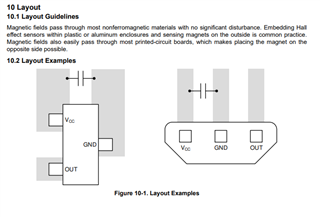
Do we have any recomended pcb layout for this sensor? If there is any can you share the details with us.

Regards

Vivek Gandham. 

  • Vivek,

    Thanks for reaching out on E2E. Since this is a 3 pin device, the layout is typically very simple.  We have the following guidance in the data sheet

    With an analog output, care should be taken to avoid noise sources for the best quality measurements.  This might be accomplished by routing with ground shielding or on an interior layer away from switching signals.

    Thanks,

    Scott