This thread has been locked.

If you have a related question, please click the "Ask a related question" button in the top right corner. The newly created question will be automatically linked to this question.

DRV401: Questions of DRV401 schematics design

Part Number: DRV401

Hi Javier Sir and E2E experts,

I meet some problem when designing my circuit schematic using DRV401. Could you please give me some help?

1. My circuit is as below, Can you please help review? The main difference of my circuit to the recommended circuit from datasheet is: I add RC filter at input of the amplifier(IAIN1/2 pins) to filter the PWM ripple. Is this OK?

2. Do I need to supply DRV401 using a Linear Regulator power? Or my Switching Power supply (About 30mVpp ripple at 600kHz)is fine? my fluxgate runs at 450kHz to 490kHz.

3-1. Confused of the diode: I find only 1 steering clamp diode is used in Figure 8 Basic connection circuit in DRV401 datasheet. Do I need to put a steering clamp diode in every ICOMP1/2 pin?

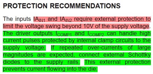
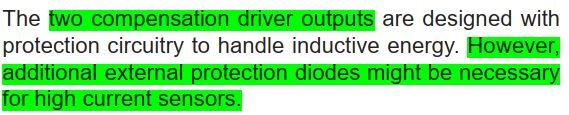
3-2. Confused of the diode: I have thought the diode is used to protect the IAIN pin against the High voltage from compensation coil(as the description in red color background shows). However, I find the diode is used for protecting ICOMP1/2 pins indeed(as the description in green color background shows):So, whether the diode is used to protect IAIN pins or the ICOMP pins? Why ICOMP pins need to be protected?


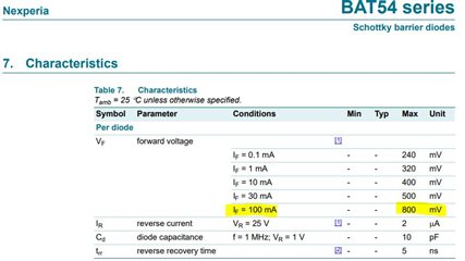
3-3: What kind of diode to use? it recommended me to use a schottkey diode in datasheet, however, the clamp voltage of schottkey diode is low,Why need I use schottkey diode here? If I have to use schottkey diode, do you have a recommended part number to share?

Thank you in advance!


Yours sincerely,
A_M

  • Hello A_M,

    1.  This is fine as the filter is also below the bandwidth of the differential amplifier.  You may be able to get better results my modifying the values of R9, R10, C3 and C4 if you are seeing noise in the PWM region.

    2.This depends on your needs.  There are 3 PSRR parameters you need to account for Offset Error, Diff Amplifier offset, Voltage Reference.  We only provide data for the differential amplifier vs Frequency.  You would need to be able to determine with your switching supply if it does not cause issue in your system.  

    3-1. The IAin2 and IAin1 are the more delicate nodes and that is the diagram only has protection on on side.  If you need protection on the IComp pins depends on the inductance and current.  The larger the current transients the more I would recommend protection on both pins. I would also move your protection to node IAIN2 instead of IAIN1.

    3-2.  The ICOMP pins have a more robust protection scheme than the AIN pins to handle some of the transients but they are limited as the size of the IC cannot meet all currents.  This is why the statement in the datasheets states if constant or large current are expected then external protection may be required.

    3-3. Here Schottky diodes are recommended as they will conduct current at lower voltages and prevent the current to flow through the DRV401 pins.  Here are some we have used previously in other devices similar.  BAT48JFILM, BAT54S(This one is Dual and easier to implement)

    Please let me know if you required further assistance or something needs more clarification.

    Regards,

    Javier

  • Hello Javier Sir,

    Thank you! This really helps me a lot.

    For BAT54S, I find its datasheet from Nexperia. It shows the forward voltage is 800mV:

    However, from DRV401 datasheet, it seems that DRV401 may have been damaged according to the absolute maximum ratings as below, because the voltage input range should below VDD+0.5V:

    It is similar to use BAT48JFILM from ST.

    My questions are:

    1. Does ICOMP1/2 pins can work with -10V to +10V voltage as the Differential Amplifier? If I understand your explain correctly, I think ICOMP1/2 should not be damaged when using 800mV diode to VDD.

    2. Can I say: the ICOMP1/2 pins are not afraid to the over-voltage, because they are output driver pins. The diode to protect ICOMP1/2 pins here is only used when current from the compensation coil is over 250mA (The ICOMP1/2 voltage is in the range of -0.5V to VDD+0.5V at the same time )?

    Great thanks!

    Yours sincerely,

    A_M

  • Hello A_M

    1. Does ICOMP1/2 pins can work with -10V to +10V voltage as the Differential Amplifier? If I understand your explain correctly, I think ICOMP1/2 should not be damaged when using 800mV diode to VDD.

    The ICOMP pins are driving h-bride and are limited to driving to VDD and GND.  They are also clamped to these voltages.  When you add the protection diodes it creates an additional path of the current reducing the current load on the protection circuit(clamps) in the DRV401.

    2. Can I say: the ICOMP1/2 pins are not afraid to the over-voltage, because they are output driver pins. The diode to protect ICOMP1/2 pins here is only used when current from the compensation coil is over 250mA (The ICOMP1/2 voltage is in the range of -0.5V to VDD+0.5V at the same time )?

    These pins are still meant to handle high current pulses but could still be damaged by large voltage as well.  The ICOMP pins can handle larger current than that of the IAinx pins.  The diode protection are also for transient on the inductor that create large voltage spikes not only larger than 250mA.  Because the inductor can create large voltage delta this could cause the input to go beyond.  The clamps will be limited and can normally handle transients.   The issue is if the application has many large transients this could weakened the clamps over time.  External clamps will share the load and improve transient protection.

    Regards,

    Javier.