This thread has been locked.

If you have a related question, please click the "Ask a related question" button in the top right corner. The newly created question will be automatically linked to this question.

AWR6843: Some questions about DMA controller

Genius 13655 points
Part Number: AWR6843

Hello Champs,

Customer has some questions about AWR6843 DMA controller.

1.  Can the DMA Port B read and write simultaneously? Or it can only read or write at a time?

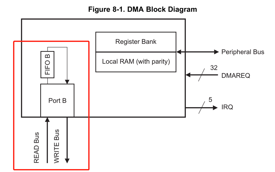
2. What does "Peripheral Bus" refer to? Does it refer to APB or AHB or other bus?

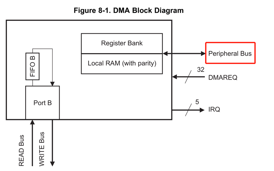
3. How does the GCTRL. DEBUG MODE bit work with CPU? Or is it only controlled by DMA hardware?

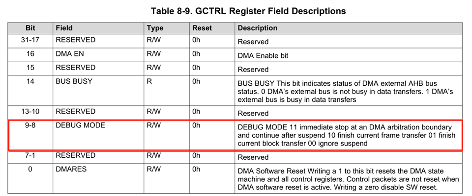
4. When is the PEND bit in channel PEND register set to "1"?

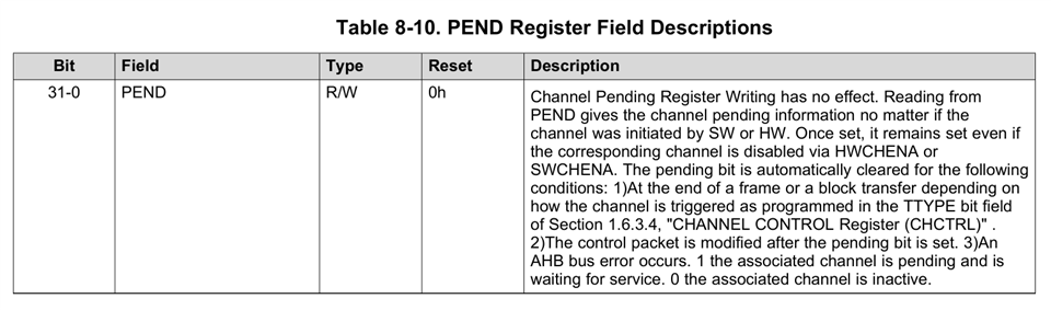
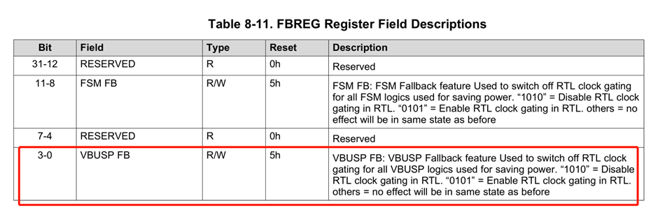
5. What is the working scheme for VBUSP FB clocking gating? Is there some relationship between FSM FB and VBUS FB clock gating?

Thanks
Regards
Shine

  • hello shine,

    I haven't received any reply yet. Would you please remind him for me? Thanks.

  • Hello Champs,

    Any suggestion on this issue is appreciated.

    Thanks
    Regards,
    Shine

  • HI, there:

    You can find some document and examples in the SDK driver directory, You will need to change the link below to match your SDK version number. 

    file:///C:/ti/mmwave_sdk_03_05_00_04/packages/ti/drivers/dma/docs/doxygen/html/index.html

    1) During each DMA channel configure, you have one source address and one destination address.  So you can only program one DMA channel to do one way data transfer.   

    Please take a look at the above document and driver examples to see whether you can find answers there for the rest of your questions.

    Best,

    Zigang

  • hi  ,

    1.  Can the DMA Port B read and write simultaneously? Or it can only read or write at a time?

    From the file you offered, I could't find any answer about whether port B can support for simultaneous reading and writing? 

    I just want to comfirm whether port B can write/read at the same time?

    Thanks

    Regards

    LS.K

  • Hi shine,

    Would you please remind him for me again?  Becaue my questions still remain unsolved.

    Thanks.

    Regards,

    LS.K

  • HI, there:

    The MSS DMA has a single port to the interconnect so Reads and Writes would not be possible in parallel.

    Best,

    Zigang

  • Hi Zigang,

    The depth of channel fifo in DMA core is just 4, so the maximum of 4 elements can be transferred one time in a channel.

    Write and read must be separated. The process of transfer should be alternated, i.e. 4 elements read -> fifo full -> then 4 element write -> fifo empty ->  then 4 element read ...

    Is this accurate?

    Regard,

    LS.K

  • HI, there:

    Not really.  Based on TRM (https://www.ti.com/lit/ug/swru520e/swru520e.pdf?ts=1687809775095&ref_url=https%253A%252F%252Fwww.ti.com%252Fproduct%252FAWR6843) section 8.1.5.3 Initial Transfer Count:  As a Single Block transfer maximum of 512 Mbytes of data can be transferred.  So you can transfer a big block of data.  

    And you can program two DMA channels.  One for read and one for write.  

    You can go through section 8.1.13 FIFO Buffer to understand the details on FIFO.  The FIFO buffer details helps you understand how multiple DMA channel switch.   But in general, it is all transparent to the users.  

    Let me know if it is helpful.

    Best,

    Zigang

  • Hi Zigang,

    Sorry, I feel confused about 

    And you can program two DMA channels.  One for read and one for write.  

    Dose it mean one FIFO can be controlled by two channels? So how many FIFO buffers are in the DMA  based on TRM section 8?

    Regards,

    LS.K

  • HI, there:

    You can program up to 64 DMA channels. Two is just an example.  And each channel you can program to transfer up to 512MByte data.   

    There will be one FIFO for each DMA engine. All the DMA channel will share this one FIFO.  Notice that only one DMA channel is actively transfer data at any moment.  DMA engine will switch between DMA channels.   

    Best,

    Zigang


  • Hi Zigang,

    So, do you mean read and write can be done simultaneously, when one channel is actived to transfer data, in order to transfer up to 512M data?

    Thanks,

    Regards,

    LS.K

  • Hi,

    Zigang is out of office today, I am forwarding this to another team member and Zigang will be returning Friday.

    Thank you,

    Angie

  • Hi, 

    thanks

    LS.K

  • Hi,

    I'm looking into this while Zigang is out. From the TRM, the maximum single "block" transfer size is limited to 512 Mbytes. A block is one or more "frames" of data. A frame is one or more "elements" of data and an element can be a 8,16, 32 or 64 word of data.

    The DMA uses FIFO B, which is 4 levels deep and 64-bits wide to read in and write out blocks of data. The FIFO operates as described in section 8.1.13 FIFO Buffer. The maximum number of DMA transactions (total reads and writes) are listed in tables 8-2 and 8-3 (depending on whether or not you are in non-bypass or bypass mode).

    Could you help us understand what the customer is trying to determine or what issue they are running into where these questions are arising?

    Thanks,

    Clinton

  • Hi Clinton,

    My question is whether port B can write/read at the same time in order to transfer up to 512M data?

    Thanks,

    LS.K

  • HI, 

    Can you explain what do you mean by read and write?    Which of the following situation you are trying to solve?

    1) Case 1: transfer data starting from address A to address B. 

    2) Case 2:  transfer data starting from address A to address B.    Also want to transfer data starting from address B to address C. 

    3) Case 3:  transfer data starting from address A to address B, also want to transfer data starting from address C to address D.

    Best,

    Zigang


  • Hi Zigang,

    It 's Case 1. During the transfer data from address A to address B, the Dma needs to read data from A and then write data from B. So I want to know whether read and write can process simultaneously.

    If they cannot be done in parallel, it is hard to transfer to 512M data in a single block. The 512M data must be splited during the transaction. The Dma FIFO depth is only 4, so the read and write must be alternated.

    However, if read and write can do at the same time, the processes of reading data from A and writing data from B are not related, but just depend on the empty/full of FIFO? Therefore, the 512M data can be transfered in a single block at one time and need not to alternate the read and write.

    Thanks,

    LS.K

  • Hi, there:

    I see.  In case 1, you can think of read and write is simultaneously.  You just need to program one DMA channel.  And you can transfer up to 512MByte data.  As I mentioned, internally how FIFO help to do the actual data transfer is transparent to the user, and you do not need to worry about it at all.  

    Best,

    Zigang

  • Hi Zigang,

    Then,I have another question about the port B. How does the Port B connect to the external Bus Matrix?  Can I understand the read and write singal wires are differently connected to the external bus, that is the read and write are controlled by two sets of control signals, such as two sets of haddr/hwrite/htrans/hsize?

    Thanks,

    Regards,

    LS.K

  • HI, there:

    Again, you can refer to section 8.1.13 FIFO Buffer in the TRM document to understand the FIFO.  Based on Table 8-2 and Table 8-3, depend on bypass or non-bypass mode, and depends on the read element size and write element size, the read/write order can be slightly different.

    Best,

    Zigang

  • Hi Zigang,

    Thanks, I have read the section 8.1.13 FIFO Buffer very carefully. In the 8.1.13, it shows how the FiFO buffer work in different element size between read(source) and write(destination). Also, it explains how to transfer different element size in bypass or non-bypass mode. However, I cannot infer that during reading(writing) data from source(destination), writing(reading) data needs to stop and wait, especially, in need of transferring 512M data in a single block.For example, if the Fifo buffer has been fulled in non-bypss mode, based on read 64bit-element size and write 64bit-element size, then one 64bit data is written to destination. Now the Fifo buffer is not full. At this moment, the read needs stop and wait until the fifo become empty, then starts to read data from source again, or it finds the fifo is not full, immediatly can start to read data from source no matter whether the write is going on or not?

    Regards,

    LS.K

  • Hi,

    Following up on this. The device is can transfer a block size up to 512 Mbytes. Is this not sufficient for the application? Is the customer running into issues while staying under this limit?

    Thanks,

    Clinton

  • Hi Clinton,

    Yeah, thanks. I want to clear about whether write(64bit element size) and read(64bit element size) can process simultaneously and need not to alternate during transferring to 512M data in a single block, and whether the read and write are controlled by two sets of control signals from external Bus Matrix during this transaction?

    Regards,

    LS.K

  • Hi,

    Has the customer observed an issue trying to transfer data with the DMA? There is sample code at the SDK install directory below. I've also listed the associated documentation that Zigang referenced above.

    <install directory>\ti\mmwave_sdk_03_06_00_00-LTS\packages\ti\drivers\dma

    <install directory>/ti/mmwave_sdk_03_06_00_00-LTS/packages/ti/drivers/dma/docs/doxygen/html/index.html

    Thanks,

    Clinton