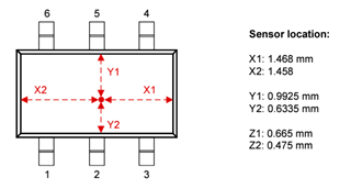
Figure 7-7 in the datasheet shows that the sensing element location inside the device.
The measurements given show that X1 (1.468 mm) is larger than X2 (1.458 mm), but the diagram suggests that X2 is larger than X1.
Is it possible that the X1 and X2 labels on the diagram are swapped, or is this simply a matter of the measurements in the diagram not being drawn to scale?