


Hi I want to inquire about PACKAGE#02 Surface Wave Artifact from PCB at
https://www.ti.com/lit/er/swrz092b/swrz092b.pdf?ts=1687374962979
If you follow the link, you will find something like this:
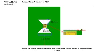
If the PCB size is large like the picture above, you will have to drill a hole. Is this really necessary?
I will use 2 IWR6843AOPs on 1 PCB for functional safety certification.
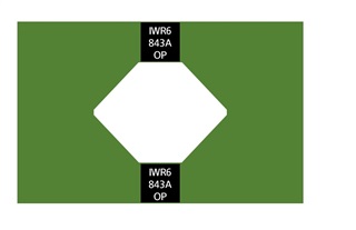
If so, it will look like the picture below. Strange shapes come out. Any other good ideas?
Actually, the reason I asked There is a difference between the TI reference board and the custom board in terms of noise.
There is a phenomenon that the custom board has more noise and cannot find the heat map.
I wonder if this is really because of the PCB shape. I'll wait for your advice.
