This thread has been locked.

If you have a related question, please click the "Ask a related question" button in the top right corner. The newly created question will be automatically linked to this question.

FDC2112: input signal

Part Number: FDC2112

Hi,

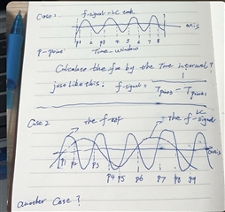
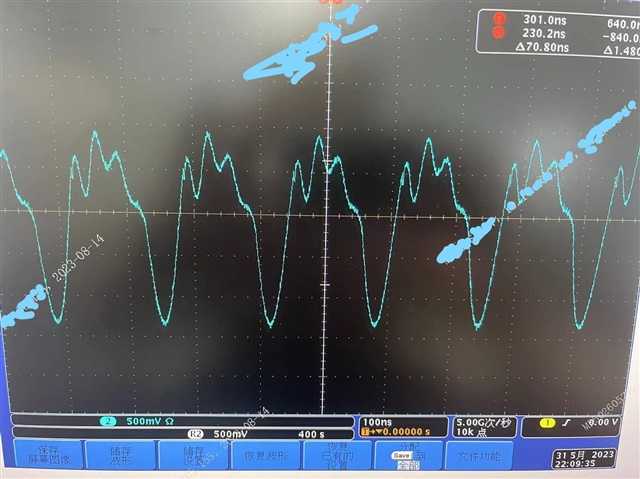
I would like to ask if the input waveform of the FDC2112 is such a signal and its positive and negative half cycle are asymmetrical, would it affect the output of the FDC2112? ,you can see it in this picture.

  • Eric,

    The sensor signal should resemble a half-wave rectified sinusoid with the minimum level being just above ground and the peak being within the range 1.2V < Vpeak < 1.8V as suggested in the data sheet.

     It looks like your waveform has > 2Vp of swing, so it might be worth reducing the IDRIVE for that channel to see if it reduces the peak voltage.

    Regards,
    John

  • Hi John

    if I use the diff mode instead of the single end mode, the input signal still needs to resemble a half-wave rectified sinusoids? can it  be a sinusoid between the diff end.and i want ask you about how  does the internal core realize frequency count?  

    Thx.

  • Eric,

    Great question. I forgot to differentiate between single-ended signals on each pin and diff signals taken across two input pins.

    I can't get in the lab at the moment to confirm, but seem to remember the INN and INP pins each have their own DC-offset, half-sinusoids time-shifted from one-another by a half-cycle.
    Taken differentially across the two input pins, you should see a full sinusoid swinging about about zero volts.

    The device determines the frequency by comparing the elapsed time of the sensor signal's axis crossings to a reference clock.
    Please see equation (8) in the FDC2112 data sheet.

    Regards,
    John

  • Hi John,

    I got it, but i want to ask a new question about the input is an asymtemetric  signal ,the negative half wave is  not as the as the positive half. does it matter in diff input mode? will it affect the measure result?

  • Eric,

    The asymmetrical shape may indeed affect the results, particularly since the upper half of the waveform appears to have a different duration than the bottom half of the waveform.

    But before we take that much further, can you probe the two pins single-separately - showing the ground references -  and post the waveforms to this thread?

    Regards,
    John


  • Hi John,

    I,m  sorry for getting back to you late but after i discussed with the engineer, I have know the actual problems,

    first of all, can you help me to check  how the core calculate the input signal frequency just refer my hand script (picture 1). can you show me more about this?

    the second is the input signal just like the upload picture before. that is the actual signal they tested, for the input signal ,we can see the up half wave has some spurs, but if they  increase  the input signal's amplitude to 2 voltage even more, the output keep stable, but if they change the input signal's amplitude to 1.2v-1.8v,the output will jump random. so we guess that when the input signal amplitude large enough ,it will beyond the acquisition zone(1.2V-1.8V),and  the original signals will be sampled in the  fixed point as the normal signal just refer the picture 2

    Thx.

  • Eric,

    Thank you for the additional information.
    The FDC2112 is counting axis crossings of a sensor signal that should look like a sinusoid when measured differentially across the input pins.
    The axis crossings of the differential sensor signal are counted during an interval specified by the number of axis crossings of the reference clock as specified by RCOUNTx. As your diagrams show, the customer's sensor signal looks to have a number of sinusoids in it, and this is probably messing up the axis crossing counts.

    A few questions:
    1. In the original photo of their waveform, does the center horizontal axis correspond to ground?
    2. Can they provide a schematic and BOM of their design?
    3. What waveforms do they see when they probe the two input pins separately?
        Can they provide snaps of those signals?
    4. Are they using a 40MHz external reference clock? If they are, can they verify it is clean and stable?

    Regards,
    John

  • Hi John,

    In the actual use process, the baseline of the signal is below 0V, -0.2V or so, they have tested, it is indeed due to waveform distortion caused by the measurement results are wrong. The measurement waveform distortion is caused by the addition of EMI filtering to the signal input, remove the EMI filter circuit, the input signal is a perfect sine wave, and the test result is correct. Secondly, I want to understand the specific method of signal crossing the axis, is it like I described? If so, how to quantify the exact location of the intersection. Second, customers can ensure stable output by increasing the amplitude of the input signal. The customer wants to know where the specific internal crossover occurs, and whether it can ensure stability if the signal amplitude exceeds (1.2V-1.8V) and works for a long time.

  • Hi John,

    i want konw how the axis corssed by the input signal is a baseline (the axisjust like a x axisand it's about  0v or another direct voltage?)can you show me how the signal cross the axis.this may influent the follow steps we need to act.and i want to have a webex meeting with you ,can we shchdule a claendar.

    Thx.

  • Eric,

    The device looks at the differential input waveform as it crosses thru GND.
    So GND is the crossover.
    The amplitude range is specified so as to make sure the SNR is high enough to give reliable detection.

    Regards,
    John

  • Hi Jhon,

    Thank you for your response. I got it. I have another question about this chip, if the signal amplitude exceeds 1.8V(1.8V -VDD), if the chip will be destroyed for a long time in this case ? 

  • Eric,

    A higher voltage will not damage the chip.
    The most likely complication is the waveform may clip and that could reduce the device's accuracy.

    Regards,
    John

  • Hi John,  I've been reading some of these other threads and I have a question here. 

    You mention that the device is measuring the axis crossings at ground 0V. You also say that increasing the amplitude of the waveform may cause it to clip and reduce the device's accuracy.  If the waveform is increased and it starts to clip, I would assume it would look square, with only the 2 certain crossings of the axis per period.

    Could you explain a bit more as to why the larger amplitude could reduce the device's accuracy?

    Thanks,

    Hadyn

  • Haydn,

    In a theoretical sense, the clipping shouldn't matter and the distortion caused by the clipping shouldn't impact the axis crossings.
    But these devices are sophisticated mixed-signal chains in their own right, and there's a lot going on inside of them.
    There are all kinds of limiting, amplitude control and level shifting going for a variety of reasons.
    And these things are critical to protect the device from excessive input voltages and preserve the signal's integrity as it works its way thru the device, all the while keeping precision at a desirable level.

    Hard clipping can throw those things off and the resulting internal distortion can hurt precision & accuracy.
    That's one of the reasons we publish input voltage limits in the data sheet.

    Regards,
    John

  • Hi John,

    The customer is currently asking a question about the FDC2112 and they want to know what exactly this 0V reference line, which is the baseline through which the oscillating waveform travels in a differential application. Is the GND signal? But in a differential application, our power supply is only positive, no negative voltage, so how do our internal circuits capture a negative signal, At this point the crossing reference line is 0V or 1/2VDD ?

  • Eric,

    The device applies internal gains and level-shifting of the signals at the input pins as part of the analog processing.
    There is most likely an internal, non-zero voltage that is used as the reference point for axis crossings.

    Regards,
    John

  • Hi Jhon,

    I would like to ask the customer whether we can know exactly what the level is and whether there is a formula to calculate it. Also for single-ended and differential applications, the differential signal has a positive and negative half cycle and the chip is powered from a single power supply. how negative signals are captured inside the chip. If the level is passed, is the level automatically adjusted internally? 

    Thanks

  • Eric,

    After reviewing the original design reports, the differential input is changed to an (almost) digital waveform that is interpreted as a sensor "clock" signal that is counted over a time window determined the reference clock and some some device settings, like RCOUNT_CHx, CLOCK_DIVDERS_Chx etc. 

    After this point, analog is used only to control the sensor signal's amplitude, and not anything in the frequency or time domain.
    Any details beyond this are considered proprietary.

    Regards,
    John

  • Hi Jhon,

    First of all, thank you very much for your reply. For me, I already know a lot about the use of this chip. but you also need to know some of the details that you're talking about. For the internal count you're talking about, I already know that it's going to be in a fixed time window to calculate the number of times the LC oscillation signal crosses the reference reference baseline, and so I'm going to get the frequency of the oscillation signal, but I need to have an absolute definition for the specific value of the reference baseline. For example, in the case of differential inputs, is the reference line referenced to (Vdd/2) or GND? For single-ended input, is the signal cross GND or a fixed DC level as a reference line? At this time, the customer is very concerned about this issue, so I look forward to your response. We would rather get an exact answer.

    Thanks,

    Eric.

  • Eric,

    It is best to assume it is always refenced to ground.

    Regards,
    John

  • Hi Jhon,

    For the differential mode, the signal must have the positive half wave and the negative half wave .for the core, how it can sample a negative signal if there is any internal charge pump used to provide a negative power supply for the chip and  I think the GND reference line just like a comparator ,once the signal cross the GND,there will be a signal change just like rising edge or falling edge .if the internal works like this ,i need to know the comparator is a zero-crossing comparator or a hysteresis comparator?if it is a hysteresis comparator ,what is its tolerance range, the reference line's  vlotage level may not be a absolute value. 

    Thanks.

  • Eric,

    The two device input pins are connected to a zero-crossing comparator, with the 'A' device input on the comparator's positive input, and the 'B' pin connected to the comparator's inverting input. The comparator's output is differential, so during a positive cycle on the 'A' input (with the 'B' input at ground), the comparator's positive output is HIGH, and the negative output is LOW. For a negative half cycle (a positive input on the device 'B' input, with the 'A' input at ground), the comparator outputs are opposite. 

    All of the analog signals are referenced to ground.

    The comparator represents the boundary between the analog and the digital domains, so after the comparator, the processing is all digital, including the zero-crossing detection.

    Regards,
    John

  • Hi Jhon,

    but for the negative half wave ,how it can sample such a signal ,the signal just have a positive power supply,unless there is a charge pump used to generate a negative power

  • Hi

    The Vin(Voltage on any pin) written by FDC2112 does not exceed VDDHeavy plus sign0.3 (3.3V power supply, so this voltage is 3.6V)

    Based on the internal principle of this chip, for the two pins of differential input, does this voltage mean that the peak of the differential signal does not exceed 3.6V, or does it mean that the single-end ground-to-ground voltage of the differential pin does not exceed 3.6V? Please confirm this problem. Thank you.

  • Eric,

    The Absolute Max rating spec means the voltage on any pin with respect to ground should not exceed VDD + 0.3V.

    Regards,
    John

  • Hi Jhon, is there any charge pump in chip ?if there is no ,how the chip can sample the diff signal ,the diff signal has both the positive and negative half wave.

  • Eric,

    The signal is not conditioned by a charge pump.

    The input drives a fully differential comparator, which translates the analog input into the digital domain, where the axis crossing counts happen.

    The sensor waveform's half-cycle on INxA (while INxB = 0V) goes to the comparator's non-inverting input and forces a HIGH on the comparator's output: VOUT(OUTP,OUTN) = HIGH.

    The half cycle on the INxB input pin (which actually has a positive polarity while INxA = 0V) goes to the comparator's inverting input pin, and forces a LOW on the comparator's differential output: V(OUTP,OUTN) = LOW.

    So the two separate half-sinusoids on the two input pins do end up looking look like a ground-referenced full sinusoid when the inputs are examined differentially. It is easy to think this sinusoid moves thru the chip as an analog signal, but in fact, it does not. Once the analog signals arrive at the comparator, they are converted into digital pulses, which strips off the analog information, but preserves the timing of the axis crossings, which is the critical information.

    After that point, the digital core counts the axis crossings and does the conversion over a time window controlled by RCOUNT and other parameters. 

    Regards,
    John