We are using the FDC1004 for level sensing and are experiencing a few challenges. We have designed our system In accordance with the
https://www.ti.com/lit/pdf/snoscy5
Application note : SNOA925
Similarly, we have used the out of phase technique for level sensing where we have our CH1,CH2,CH3 in phase with Shield 1 with Shield 2 being use for out of phase excitation. Our PCBA stack-up is as follows: Coverlay Insulator/Shield/Dielectric/Sensor plates(Ref. air, level ,liquid))/ Coverlay Insulator/Adhesive .
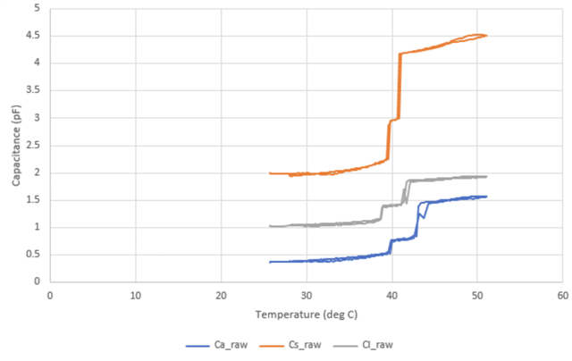
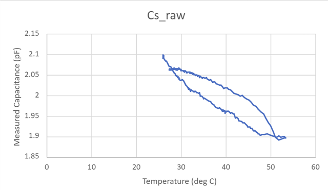
We observe an offset error between 0.966 to 2.718 pf across all channels with a 30 deg C temperature rise (between 20 to 50C). The absolute offset error is proportional to area of the electrodes.
Note that the effect occurs when heating the FDC1004 locally, not the electrodes.
According to the datasheet FDC1004 4-Channel Capacitance-to-Digital Converter for Capacitive Sensing Solutions datasheet (Rev. B) we were expecting to observe around 0.1 % of drift in capacitance readings.
In our previous design attempt for level sensing ,we had used a grounded EMC film on top of the shield but removed this as we were loading the shield drivers above spec. With this design we observed a gain error of 10-20% of capacitance across all channels with a 30 deg C temperature rise. We suspected this may be due to the extra loading on the shield driver and hence why we removed it.
Does TI have any explanation on why exactly could we be observing an temperature related offset error on the channels?


