This thread has been locked.

If you have a related question, please click the "Ask a related question" button in the top right corner. The newly created question will be automatically linked to this question.

LDC1614: LDC1614RGHR: I2C strange behavior

Part Number: LDC1614
Other Parts Discussed in Thread: TCA9416

Hi

I have a PCB which uses a NFC tag as a I2C bridge for communication and power supply to the LDC1614RGHR sensor. I have only one master (tag) and one slave (sensor) at the I2C lanes. If I use an external power supply for the sensor and the pullup resistors (while the NFC tag feeds itself, VCC = VOUT = 3.0V) everything works fine, the signal gets tunnled and it is possible to read out values from the sensor through I2C.

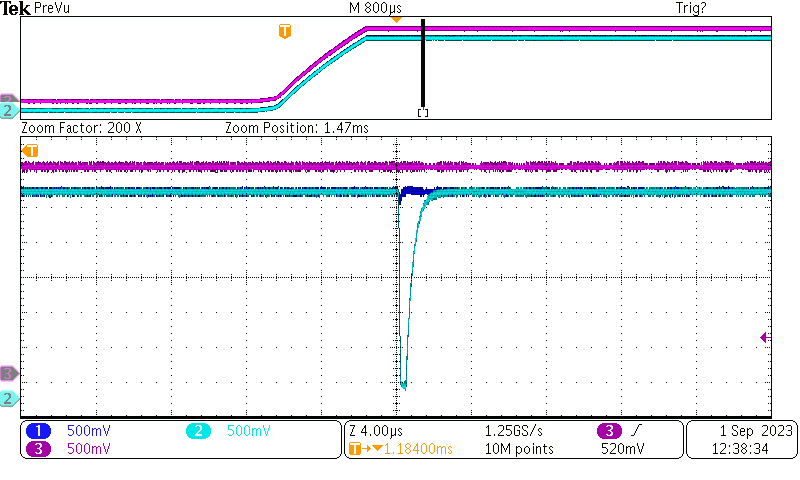
If I feed everything from the tag (VOUT = 3.0V, Iload = 1.4mA, field to the coil more than strong enough), I get no working communication. The tag don't clocks the SCL or SDA lane, both are the whole time just high.

If I cut physically the LDC1614RGHR sensor away (pullups feeded from energy harvesting from the tag) and start a communication with the sensor, I can see that the tag (master) starts the communication with a start condition and the slave address but receives no ACK, what make sense, there is no slave. But the communication starts correct.

The firmware code is in all three cases exactly the same. Also is the load current identical and I can't see any dips in the voltage supply or something like that. It seems to me like a stucked I2C bus (if I supply the whole circuit from energy harvesting) but with SDA and SCL constant high, that should not be the case...

My question is, how is it possible that the master sends nothing to the bus (not even the SCL clocks) if there is a LDC1614RGHR on the I2C lines and is feeded not from a lab power supply? Are there any known issues with the LDC1614RGHR sensor which could explain this behavior?

Best regards
Raphael

Picture 1: The whole circuit

Picture 2: Communication if I cut away the sensor

  • Hello Raphael,

    This issue seems similar to a floating GND, SD, or ADDR pin.  Can you take a look at those pins on the oscilloscope during power on and I2C communications?

  • Also, I see in your schematic that there are no pull up resistors on SDA/SCL.  These are required for an open drain IO, such as I2C.

  • Hello Eddie

    I forgott the pullups in the schematic that I post, but in reallity they are there (both 5.6kOhm to 2.8V). What is very strange to me is that if I supply the whole circuit from a lab power supply, the master clocks the SCL line, the sensor give me an ACK and I can read from all registers. If I supply everythin from the master (NFC tag with power harvesting), the master can't get a communication to the sensor (the MASTER don't even produces SCL clock pulses, SCL and SDA are both the whole time high). If I supply everything from the master and remove the sensor, the master clocks the SCL line correct. For me it looks like the sensor stucks the bus in a magical way (but both I2C lanes are constantly high).

    I measured the GND, SD and ADDR pins with the osciloscope and i can't see anything scarry.

  • Raphael,

    Thanks for the update.  Another thought I had was a potentially slow slew rate on the supply.  This is not an issue we have run into before with this device, but if the slew rate is very slow or droops during the ramp up, I could possibly see an issue with proper power up.  Since the only change is the power supply, there is likely something related there. 

    I am not sure the details of how the NTAG device works exactly, but if there is a varying RF field, the power could be inconsistent.  It would be good to also see the power up ramp.  You could possibly also duplicate the ramp with a bench supply.    

    Also, you have the SD pin tied low.  This powers the device up in active mode which has typical current draw of 2.1mA, not including sensor current or pull up resistor current draw.  The pull up resistors are also about 500uA(2.8V/5.6k).   


  • The supply seems totally proper for me, I added a picture of the slew rate at the supply startup of the NFC tag. Also, there are no dips, or something:


    We used in another attempt a lab supply in parallel with the supply from the tag and a diode/resistor in between, so the supply from the tag should get assisted (and with this be unaffected from possible RF field fluctuations) but it doesn’t work with the same failure as if we use the tag supply solely (not even clock cycles on the SCL, SCL and SDA the whole time high):

    Supply currents of 2.1mA + 500uA should be no problem, the tag supply at maximum a current of 10mA @ 3.0V


    If I read the datasheet of the LDC1614 under "7.5.2 Pulses on I2C" I ask myself why Texas write that into the datasheet? It seems to me that there were problems with the I2C communication in the past in other cases?

  • Raphael,

    Thanks for the additional data.  I agree, that the power ramp looks okay without dips. 

    10mA @3V seems like a large amount of power to harvest from the NFC field unless the reader is fairly powerful.  From my past testing, readers such as NFC enabled phones would typically achieve a couple mAs.  Larger current and range was achievable only with high power readers and larger antennas.  May be worth looking into just to be sure you are getting the power expected.  It does not appear there is a current draw issue from the power ramp shot you showed though.    

    You could try a test where you power up the tag from the RF field with LDC disconnected, then connect LDC and try to initiate communications.  This may help to point whether this is a problem during power up.   

    This is a kind of a strange issue, so I am still thinking about other considerations as well.

  • The power that is harvested from the NFC is definitively not the problem, I measure the max. harvested power with our exact setting: 17mW @ 3.0V -> 5.66mA

    If I disconect the LDC completely (SCA, SCL, VCC) and supply everything from the NFC power harvesting tag, then I have the same problem -> no communication is possible and the master can't send SCL clocks. If I hold the LDC connected on the supply line and disconnect during the startup of the VCC line only SDA and SCL, then I get a working communication after I connect the I2C lines. If I look at the SDA and SCL lines at startup of the supply, I see that they go both at the exact same time to the high state (which makes sense because the pullups get supplyed). Maybe that is a problem for the LDC. So I guess that is a glitch inside the LDC I2C module.

  • Hi Eddie

    I have to correct myself, the problem is not that the SCL and SDA lines at startup are at the same time high (through the pullups), the problem is that the LDC (slave) sends a start condition (SDA goes from high to low during a SCL high) after power up. Our tag (master) thinks after the start condition that another master is on the bus and don't produce SCL clock cycles when we send a regular command because he thinks he is a slave:

    pink: VCC at startup

    light blue: SDA line

    dark blue: SCL line

    Our solution is that we insert a I2C isolator IC (TI TCA9416) between the tag and the LDC and isolate SDA and SCL during VCC startup and 10ms after. But for sure, I think this is a glitch inside the LDC I2C module. Thanks for your help :-)