

Hi TI
I would like to make some inquiries for IWR6843AOP custom board layout.
1. How should my customer deal with the PCB pattern on the IC Bottom surface?
- Do they just need to process GND? Is there any additional work needed for heat dissipation?
- Should GND be processed and soldered?
(Looking at the IC sample, it doesn't appear to be soldering)
- Should IC Bottom Side PCB be free of copper foil?
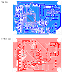
2. They proceeded with PCB Artwork as below first, and it is PCB 2 Layer.
Should they separate GND into Analog GND and Digital GND as shown in the picture below?
Please answer to the questions regarding GND handlinig in PCB Layout
Thanks.
Regards,
Jack
