This thread has been locked.

If you have a related question, please click the "Ask a related question" button in the top right corner. The newly created question will be automatically linked to this question.

FDC2214EVM: FDC2214 Dead Zone

Part Number: FDC2214EVM
Other Parts Discussed in Thread: FDC2214

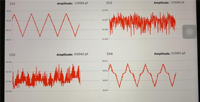
Hi, we have designed a capacitance sensor board using FDC2214 following the FDC2214EVM schematic. During testing we found there are dead zone of data read from FDC. The below graph shows what we observed.
The same triangle shaped signals are input to both ch2 & ch4, the graph is draw directly from data out from FDC's ch2 & ch4. We'd expect ch4 drawing shall be the same as ch2 in triangle shape. It seems there is a dead zone in ch4. 

What could cause this phenomena? How do we remedy this, or any solutions to this?

Thanks!

  • Yanbing,

    1. What is your test set-up?
    2. What test conditions cause the dead zone?
    3. What does the device behavior look like outside of the conditions that cause the dead zone?
    4. Can you share your PCB layout?
    5. Is it possible to probe the sensor waveforms with a high impedance probe for conditions (2) and (3) above?
      if the waveforms do not look sinusoidal, try probing with a leaded 1k resistor between the probe tip and the PCB test point.

    Regards,
    John

  • John,

    Thanks for answering me back. Answers to your questions:

    • A1: See below.
    • A2: See below.
    • A3. Outside the dead zone, the output drawing should be the same shape as input waveforms. In the picture of my first post, the ch2 drawing shows the normal condition. It is the same shape as the input triangle waveform.
    • A4: We recreated the phenomena on TI FDC2214EVM board, https://www.ti.com/tool/FDC2214EVM?keyMatch=FDC2214EVM.
    • A5. We use signal generator to produce regular waveforms, found the triangle shape can best show the dead zone phenomena.

    Description of our test:

    • We found the problem first on our own boards, then we recreated the phenomena on the TI FDC2214EVM board.
    • The test is setting up 4-channels sampling sequentially at 100Hz frequency, which is our application requirement.
    • A MCU reads out raw-data and the plot as you see in first post. The initial register values are as following:

    static const reg_val_pair_t fdc_config_multi_channel[] =
    {
        [0].reg = FDC_CONFIG_REG, [0].val = 0x3E01, // chn|slp|lp|CLKIN|intb|lowc, F_clk=40MHz
        [1].reg = RCOUNT_CH0_REG, [1].val = RCOUNT_MULTI_CHANNEL, //0x186A, Tc = (0x186A * 16 + 4)/F_ref = (0x186a*16+4)/40MHz=2.5ms
        [2].reg = RCOUNT_CH1_REG, [2].val = RCOUNT_MULTI_CHANNEL,
        [3].reg = RCOUNT_CH2_REG, [3].val = RCOUNT_MULTI_CHANNEL,
        [4].reg = RCOUNT_CH3_REG, [4].val = RCOUNT_MULTI_CHANNEL,
        [5].reg = SETTLECOUNT_CH0_REG, [5].val = 0x0060,  // Ts0 = (0x60*16)/F_ref = 0x600/40MHz = 38.4us
        [6].reg = SETTLECOUNT_CH1_REG, [6].val = 0x0060,
        [7].reg = SETTLECOUNT_CH2_REG, [7].val = 0x0060,
        [8].reg = SETTLECOUNT_CH3_REG, [8].val = 0x0060,
        [9].reg =  CLOCK_DIV_CH0_REG, [9].val  = 0x2001,  // fin_sel=b10, fref_div=1, F_ref=F_clk/fref_div=40MHz
        [10].reg = CLOCK_DIV_CH1_REG, [10].val = 0x2001,
        [11].reg = CLOCK_DIV_CH2_REG, [11].val = 0x2001,
        [12].reg = CLOCK_DIV_CH3_REG, [12].val = 0x2001,
        [13].reg = FDC_MUX_CONFIG, [13].val = 0xC20D, // auto-scan=1, RR_Squ=b10:chan[0,1,2,3], deglitch=b101:(10MHz)
        [14].reg = DRIVE_CURRENT_CH0_REG, [14].val = 0x5400,    //Idrive=b01010: 0.069mA, so sensor amplitude: 1.2V~1.8v
        [15].reg = DRIVE_CURRENT_CH1_REG, [15].val = 0x5400,
        [16].reg = DRIVE_CURRENT_CH2_REG, [16].val = 0x5400,
        [17].reg = DRIVE_CURRENT_CH3_REG, [17].val = 0x5400,
        [18].reg = FDC_ERROR_CONFIG_REG, [18].val = 0x0001, //DRDY_2INT
    };

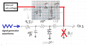
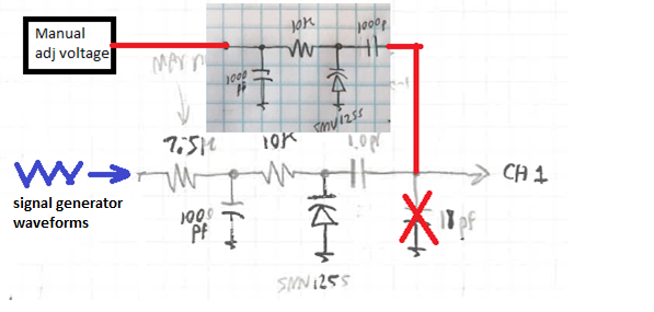
    • We made a simple circuit using varactors to generate input signals, to feed into input channels on FDC2214EVM board. A hand draw schematic as below:

    • The signal generator output waveform: amplitude=~200mV, offset=1.5V, frequency=1Hz.
    • The red line input in above diagram can manually adjust the average capacitance. This is how we found the dead zone.
    • We found dead zone in all 4 channels, while ch1/ch2/ch3's dead zone seems at same spot, but ch4 dead zone is at different spot.
  • Yanbing,

    The capacitive sensor should interact with the on-board inductor (and any capacitors & parasitics)  to form an LC resonant circuit, which is the basis of the oscillator. 

    If everything is working right, the waveform at one input  pin should look like a half-sinusoid going from ground to a peak voltage between 1.2V and 1.8V. 
    The other pin should also look like a half-sinusoid, but it will be displaced from the other pin by a half-cycle.
    Taken differentially, the input waveform should look like a full sinusoid passing through 0V, with a peak-to-peak amplitude between 2.4V and 3.6V.
    The frequency limits for the input waveform are 10kHz to 10MHz.

    Is this wat you are seeing with your device in and outside of the dead zone?

    Regards,
    John

  • John - Hi, I'm also working on the same FDC2214 program with Yanbing. Thought I'd jump in to provide the bigger picture and a few more details. Sorry for the extended length of this writeup. 

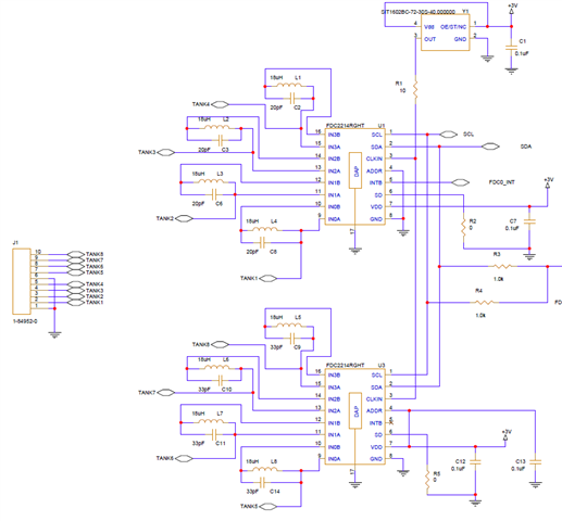
    We are using two FDC2214s to measure the capacitance values coming from an 8-input capacitive sensor. This sensor measures health-related waveforms (pulse, blood pressure, heart rate, etc.) in real time. The basic measurement concept has already been proven on previous revisions of this product using the FDC2214. In other words, we already know the FDC2214 is capable of handling these capacitive waveforms without aliasing or loss of fidelity. The capacitive sensor signals (connector is on left) are referenced to ground. We use a 40 MHz external clock for frequency discrimination. Tank inductance is 18 uH. The relevant portion of the schematic is shown below. It's pretty standard and per your DS. 

    We are now working on a new revision of this product. Because it is difficult to get repeatable measurements with the capacitive sensors, we have been using a dual varactor circuit to emulate the sensor's capacitance as a function of time. This makes for simpler and consistent measurements. Here's a hacked-up schematic for that circuit. 


    The top-most varactor sets the 'average' capacitance for this sensor emulator. We can adjust that average capacitance with a DC supply. The bottom varactor is modulated with DC + a 1 Hz triangle waveform. This triangle wave mimics a real-time telemetry signal from the patient and allows us to measure the capacitance variations as a function of time.  

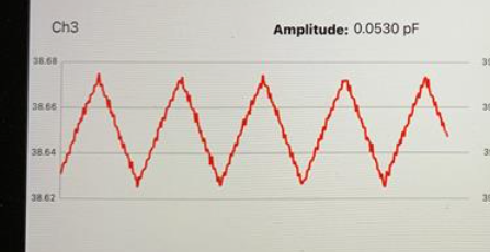
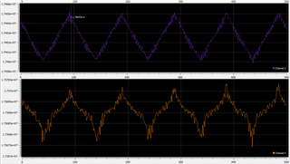
    With one input going into one FDC channel, we see the crisp triangle waveform shown below (CH3). [This waveform is provided by our application. It is derived from the DATAx output of the FDC.]

    However, when we extend this setup from one to two channels (in other words, we attach separate capacitance generator circuits to two FDC channels), we get the following outputs.

    Channel 3 (CH3) is still pristine but CH4 now has a dead-zone at the signal midpoint. Note that we can change the value of this dead zone by varying the average capacitance of the top-most varactor in our generator circuit. This fact is telling me something - but I'm not sure what. 

    The channel choices don't have to be sequential to show this good-bad behavior either. Here CH1 is perfect and CH4 shows the dead-zone behavior. (CH2 and CH3 had no sensor inputs). 

    We are perplexed by this behavior and just need some help in troubleshooting the issue. We seem to get this right when using one channel. Going to more than one channel is giving us problems. Any ideas?

  • mark,

    Many thanks for the thorough description.

    While we dig into this, some initial questions:

    1. I'm not sure if this makes sense, but does the order of the sampling matter?
      If you start with CH4 and alternate with CH3 do the results change?
    2. If you switch the varactor input circuits, but keep the sampling the same (CH3-CH4), do the results change?
    3. Are the conversion & drive-related register settings for the two channels identical?

    Regards,
    John

  • All good questions. I can answer question 2 in the lab pretty easily. I'll get on that right now. 

    I'll ask Yanbing about 1 and 3. Thanks very much. 

  • John,

    I replied directly via email, but it did not show up here, so I re-enter here.

    Let me answer your questions #1 & #3.

    Ans1: Are you referring to sequence order of sampling of ch1 through ch4? I am not sure if there is a way to control that in software. Or do you mean we provide test signals in different order? If yes, I am sure it does not matter the order of which channel gets input first, the same phenomenon can be observed.

    Ans3: the register settings are identical among all four channels.

  • Thank you Yanbing.

    Ignore that first question. It was not well thought out.

    The figure below is from the data sheet. For single-channel mode, the lower trace shows a single start-up or activation time, followed by successive conversions. In your plots. the output from this scenario looks okay.
    The upper trace shows sequencing between two channels with where each channel has an activation time, followed by conversion and a switch delay. 
    The activation time  allows the sensor to stabilize after oscillator start-up:

    (6)     tsx = (CHX_SETTLECOUNT × 16)/frefx

    Since the problem appears for a multi-channel scenario and not a single channel, then it seems the activation time may be something worth checking.
    Regards,
    John

  • Include figure mentioned in my last reply:

  • John,

    Maybe there was in-accuracy in our earlier descriptions, we observed the dead-zone in single channel case too. The FDC is programmed always collecting 4 channels in sequence, and repeating in100Hz frequency. We can observe dead zone even with only one channel is input with varactor modulated signal.

    For your time questions. In our application, there are 2x FDCs collecting 8-channels., so it means ~2.5ms per channel time. The registers RCOUNT_CHx = 6250 for conversion time, and SETTLECOUNT_CHx = 96 for activation time.

  • John - sorry for my inaccurate statement about seeing the dead zone in single channel use. Yanbing is right - It happens in single channel mode too. 

    I also apologize for the piecemeal nature of the information we're providing. We're gathering information in real time on the bench and what seems like solid clue one day appears to be unrelated a day later. Here's what I noted yesterday. 

    • As we adjust the average capacitance of our triangle wave varactor circuit, we can present certain specific values of input capacitance to the FDC that produce the dead zone in our triangle wave output. 
    •  Those dead zone values of capacitance appear to be fairly consistent over multiple channels and over at least a few units.
    • One such dead zone value is 20.446 pF. This value is very repeatable in the units we observed. 
    • This capacitance value translates back to a tank frequency of 8.2962093 MHz (assuming 18uH nominal capacitance). 
    • this odd frequency does have one interesting quirk. 135*Ftank is equal to 28*Fref to within 10ppm. [note that Fref is 40 MHz.]
    • This could be telling us something - the values are pretty precise. Or it could just be an absurd coincidence.  
    • I can find other average input capacitance values that produce the same dead zone in our triangle wave output. Those values don't translate to frequencies that have the interesting mathematical equivalence noted above, but they are repeatable. 
  • Yanbing,

    Thanks for the add'l info.

    Does a single channel always show a dead zone, or are there special conditions?

    What do the sensor signals look like on INxA and INxB with and without a resulting dead zone?

    The two pins should look like half-sinusoids with a minimum near GND, peaks between 1.2V and 1.8V, and  their timings should be displaced from one-another by a half cycle. The differential voltage between the two pins should look like a full sinusoid about GND.

    Regards,
    John

  • John,

    Dead zone can always be observed, either single channel or multiple channels. There seem no special conditions. 

    One observed phenomena as Mark described, under the same test setup, when dead zone appears, the capacitance value at the dead zone are always the same, among deferent channels of same device, as well as among different devices. On a different test setup, (since Mark is located in Atlanta and I am in Dallas), the same phenomena can be observed, i.e. the capacitance values at the dead zone, are same among different channels, as well as among different devices. But My observed capacitance value is different from Mark's.

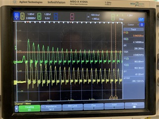
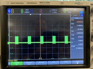
    As for the sensor signals at INxA & InxB, they looked just as you described. Here are two pictures of scope, capturing IN0A & IN0B of FDC2214EVM.

    • In pic#1, IN0A & IN0B are captured with two probes, they are opposite phased, the frequency is ~4.84MHz.
    • Pic#2 shows the zoomed out of IN0B.

  • Yanbing,

    Thanks for the update. Nothing looks out of the ordinary. The zoomed-out signal looks like it might be at min amplitude, but probably is not the problem.

    If we assume the FDC and the input circuit (e.g. the varactor) is working as expected, the dead zone implies the sensor frequency is varying non-linearly, with a potential root cause being a nonlinear variation in the varactor-based input circuit.

    To this end, would it be possible to monitor/sample the sensor signal at various points in a single varactor sweep, comparing the two cases where the dead zone does/doesn't show up? 
    The main goal would be to see if the dead zone is resulting from shifts in the sensor waveform's amplitude and/or frequency.

    To illustrate the point, the images below were extracted from pictures posted earlier in this thread.
    The first image without the dead zone shows a triangle superimposed on the sweep without the dead zone; the sweep shows a relatively linear variation with no apparent dead zone.

    The second image is the same triangle superimposed over the sweep showing a dead zone. The regions of interest would be on either side of the mid-point where the sweep and triangle intersect.

    The idea would be to compare the sensor waveforms' amplitudes and frequencies at multiple points leading up to and moving away from the crossover mid-point. 

    Regards,
    John

  • Apologies, forgot to attach the images.


    John

  • John,

    We tend to believe the dead zone is not caused by the varactor, since the dead zone was observed first in a real sensor application (without varactor). To debug the dead zone, we created the varactor circuits in our labs to sweep wider ranges of capacitance to search the dead zone. With the varactor sweeping circuits we then find the dead zone using TI's FDC2214EVM board. We hope you can help to provide insights of FDC in searching the root cause or a possible work around solution.

    Above said, we are still trying to observe waveforms at multiple points along the way up to to input pin INxA or INxB, specifically around dead zone. But this appears to be very difficult, since every observation probe adds some capacitances to input channel, that affects the total average capacitance and out of range of the dead zone. We will be continuing on.

    Thanks!

  • John - we realize that the chip is what it is. If we can identify the likely mechanism for these dead spots then the hope is that we can adjust the pcb + sensor capacitance values to avoid those danger zones. We are attempting the measurement you asked for - look at INA and INB waveforms when the device is caught in a dead zone. As Yanbing has already noted, it's a little tricky as we have to compensate for the relatively large capacitive loading of the scope probes. We're on it. 

  • Hi Mark,

     I wanted to let you know that John is out of the office now.  He should be able to follow up with you next week when he is back in the office.

  • Mark,

    One of the tricks we use when observing the sensor waveform is to place a leaded 1k resistor between the probe tip and the measurement point.
    That seems to help with the extra parasitics caused by the probe.

    Regards,
    John

  • John, how are you! Thanks for your support. I have been doing a lot more testing and analysis lately. Now we have a lot more test data, and we found there are many dead zones in every channel, and they are all at same spot between channels, some are significant and obvious, some are less prominent. But it may be not so easy to describe clearly what we found in writing, I am wondering if you can have a online meeting with us, so we can better explain? A MSTeams or Zoom meeting would be sufficient. Thanks!

    Yanbing Yu

  • Yanbing,

    Our leadership's preference is to have your local TI account rep set up meetings.
    Do you have a local TI sales rep you work with?

    Regards,
    John

  • John,

    We do not have TI sales rep that I know of, we normally get our parts/boards through retailors. I am working for Murata Electronics, located in Plano, TX. Can you or your leadership recommend a sales rep for us? Thanks!

    Yanbing

  • Yanbing,

    I send you an E2E friend request.
    Please accept it and we can privately message using that app.

    Regards,
    John

  • Yanbing,

    I will close this thread for now.
    We can continue thru the messaging app or email.

    Regards,
    John

  • John,

    Thanks for you great support! Will the messaging app send mw notification email when there are updates? Anyway, we can continue with emails. Thanks again!

    Yanbing Yu