


Hi TI Experts,
I have been looking to manufacture a custom version of the Cascade radar board and would like to clarify a few things regarding the layer stack-up of the MMWCAS board. I am using Altium and found out this layer stack-up for the Revision E of the design files. I have sent the fabrication files to a vendor. The vendor says that Dielectric 2 (RO4450F) doesn't come with a thickness of 5 mil and Dk of 4.2. They told me that only Dk of 3.52 was possible with RO4450F.
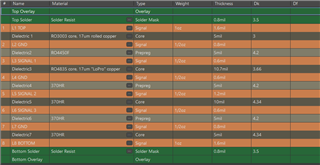
So I looked at the previous versions of the Design Files. In Revision C, I found that the Dielectric 2 (RO4450F) has a thickness of 3.62 mils and a Dk of 3.52. I believe this can be manufactured by my vendor.
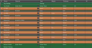
Can you please explain why this discrepancy exists among the different versions of Design Files? Can you also help me with what thickness and Dk I need to specify to my vendor so that the final design doesn't have any problems? I know that the 20 GHz signals are routed on the 3rd layer and since Dielectric 2 is directly above it, it will have a significant impact on the signals.
Thanking You
Koushal
