


Dear TI,
The MISO response for several registers listed below are not coherent with the datasheet;
- S1_CFG
- S1_S2_CFG
- DEMOD2_CONFIG
- AMUX_CTRL
The datasheet explained that data from desired address under read command is received in 2nd byte of MISO response;
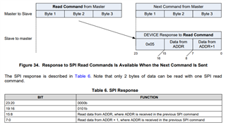
However, for the registers listed above, the obtained data of desired address from read command is received in the 3rd byte:
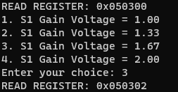
From the image shown above, read command was sent to read register S1_CFG where it is 0x050300 and the S1 gain selection was 1.67 which means the register should change to 0x050200 after write register command.
However, when read command was sent to see the update of the register after write command, the MISO response was 0x050302 which indicate that the changes was updated to the register but the data change was received in the 3rd byte of the MISO response.
Is the MISO response for the listed register behave consistent for all board of PGA970 as we have tested this issue with several boards of PGA970 at hand?

